
Pipelined parallel programming operation in a non-volatile memory system

Inactive Publication Date: 2005-03-22
SANDISK TECH LLC
View PDF10 Cites 197 Cited by
  • Summary
  • Abstract
  • Description
  • Claims
  • Application Information

AI Technical Summary

Benefits of technology

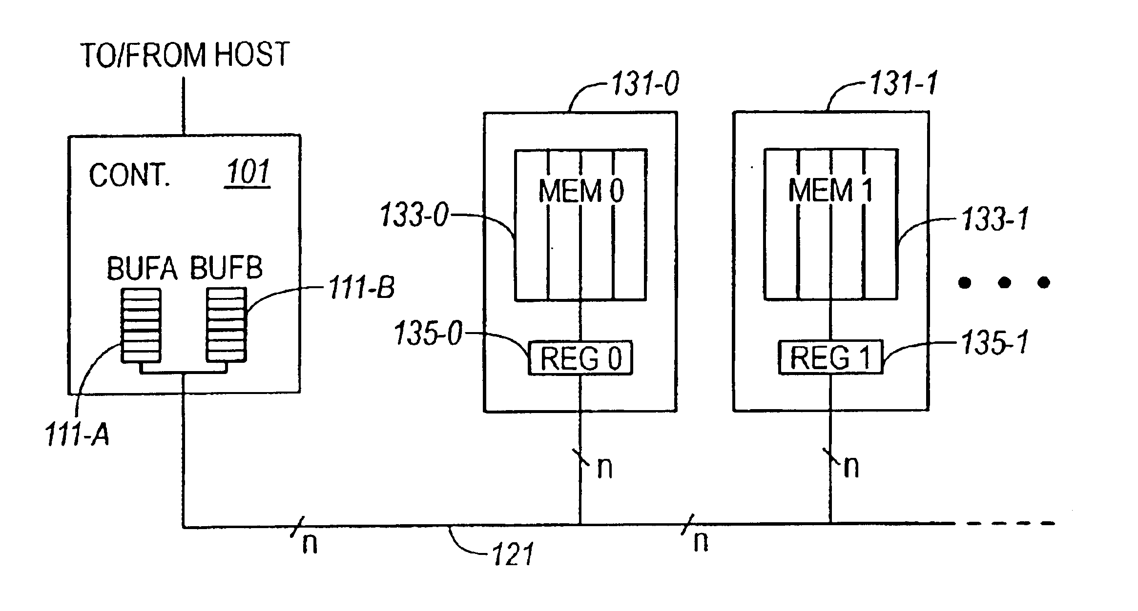
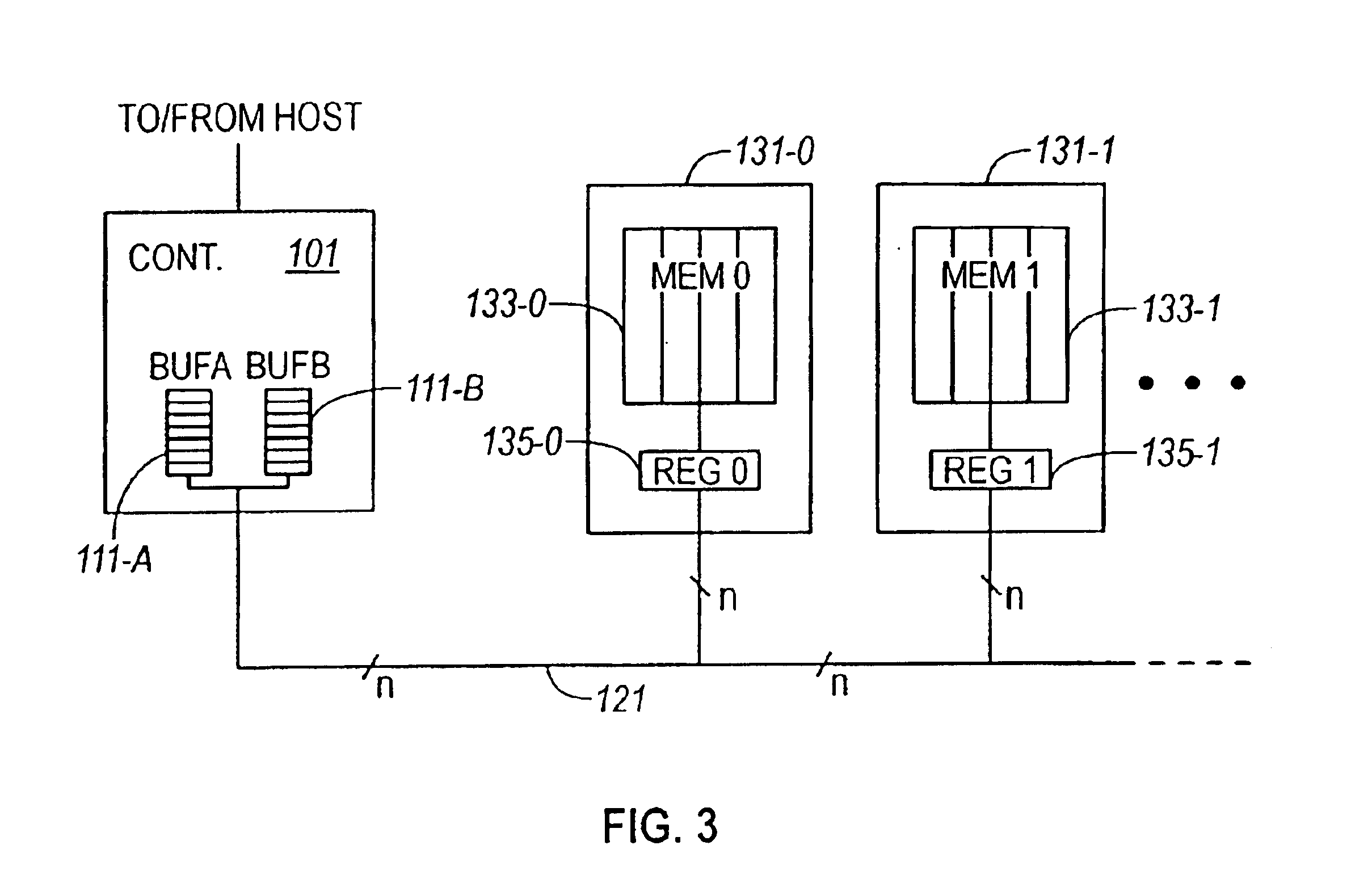
According to one principal aspect of the present invention, briefly and generally, programming parallelism in the system is increased without incurring additional data transfer latency. Data transfer and programming for multiple memory units is pipelined. Data is transferred from a controller to a first memory unit or chip and a programming operation is caused to begin. While that first memory unit is busy performing that program operation, data is transferred from the controller to a second memory unit and a programming operation is caused to begin in that unit. Data transfer can begin to the first memory unit again once it has completed its programming operation even though the second unit is still busy performing its program operation. This pipelined operation readily extends to more than two memory units. In this manner a high degree of parallelism in programming operations is achieved without incurring the latency cost of performing the additional data transfers.
In a further aspect of the present invention, two sets of embodiments are presented, one that preserves the host data in a buffer until successful programming of that data is confirmed and one that does not preserve the data on the controller. The second of these thus achieves a higher rate of data programming throughput as it does not wait for a successful programming to be achieved before reloading the buffer. In a further variation, an extra copy of the data can be maintained on the memory unit.

Problems solved by technology

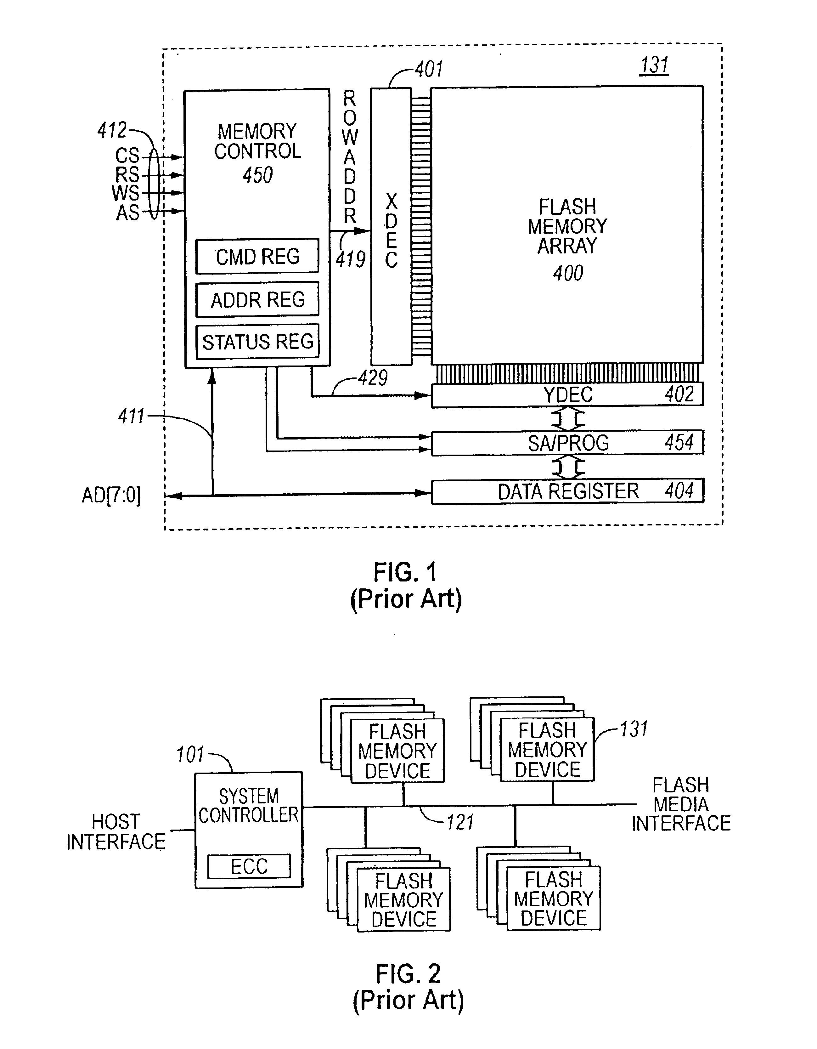
Since the programming of data into floating-gate memory cells can take significant amounts of time, a large number of memory cells in a row are typically programmed at the same time.
But increases in this parallelism cause increased power requirements and potential disturbances of charges of adjacent cells or interaction between them.
Although this increases performance, it is at the increased system cost of the multiple or wider data transfer bus.
This requires the addition of a number of pins to the controller, which increases the material and manufacturing cost of the device and also affects the resultant package size.
In addition to the practical limitations on the size of the bus, the prior art is also limited in requiring that the loading of the controller's buffers, the transferal of data to the respective registers, and the programming of the two sectors occurs simultaneously at each step in a “lock-step” arrangement that is not readily extendable to a larger numbers of sectors.

Method used


Image

  • Pipelined parallel programming operation in a non-volatile memory system
  • Pipelined parallel programming operation in a non-volatile memory system
  • Pipelined parallel programming operation in a non-volatile memory system

Examples


Embodiment Construction

The various aspects of the present invention are applicable to non-volatile memory systems in general. Although the description below, as well as that in the Background, is given mainly in terms of an EEPROM Flash memory embodiment, the particular type of storage unit used in the memory array is not particularly important in the present invention. The particulars of how the storage elements are read, are written, and store data do not enter in to the main aspects of the present invention and can be those of any of the various non-volatile systems.

In order to improve performance by reducing programming time, a goal is to program as many cells in parallel as can reasonably be done without incurring other penalties. One implementation divides the memory array into largely independent sub-arrays or units, each unit in turn being divided into a large number of blocks, as described in U.S. Pat. Nos. 6,426,893 and 6,570,785,which are incorporated by reference above. Pages of data are then ...


PUM


Abstract

The present invention allows for an increase in programming parallelism in a non-volatile memory system without incurring additional data transfer latency. Data is transferred from a controller to a first memory chip and a programming operation is caused to begin. While that first memory chip is busy performing that program operation, data is transferred from the controller to a second memory chip and a programming operation is caused to begin in that chip. Data transfer can begin to the first memory chip again once it has completed its programming operation even though the second chip is still busy performing its program operation. In this manner high parallelism of programming operation is achieved without incurring the latency cost of performing the additional data transfers. Two sets of embodiments are presented, one that preserves the host data in a buffer until successful programming of that data is confirmed and one that does not require that success be achieved and that does not preserve the data thus achieving a higher rate of data programming throughput.

Description

BACKGROUND OF THE INVENTIONThis invention pertains to the field of semiconductor non-volatile data storage system architectures and their methods of operation, and has application to data storage systems based on flash electrically erasable and programmable read-only memories (EEPROMs).A common application of flash EEPROM devices is as a mass data storage subsystem for electronic devices. Such subsystems are commonly implemented as either removable memory cards that can be inserted into multiple host systems or as non-removable embedded storage within the host system. In both implementations, the subsystem includes one or more flash devices and often a subsystem controller.Flash EEPROM devices are composed of one or more arrays of transistor cells, each cell capable of non-volatile storage of one or more bits of data. Thus flash memory does not require power to retain the data programmed therein. Once programmed however, a cell must be erased before it can be reprogrammed with a new...

Claims


Application Information

Patent Timeline
IPC IPC(8): G06F12/00G06F5/06G11C7/10G11C11/34G11C16/06G11C16/10
CPCG11C16/10G11C16/105G11C16/102G11C2216/22G06F12/00
Inventor CONLEY, KEVIN M.CEDAR, YORAM
Owner SANDISK TECH LLC
Learn More