Input/output buffer
- Summary
- Abstract
- Description
- Claims
- Application Information
AI Technical Summary
Benefits of technology
Problems solved by technology
Method used
Image
Examples
Embodiment Construction
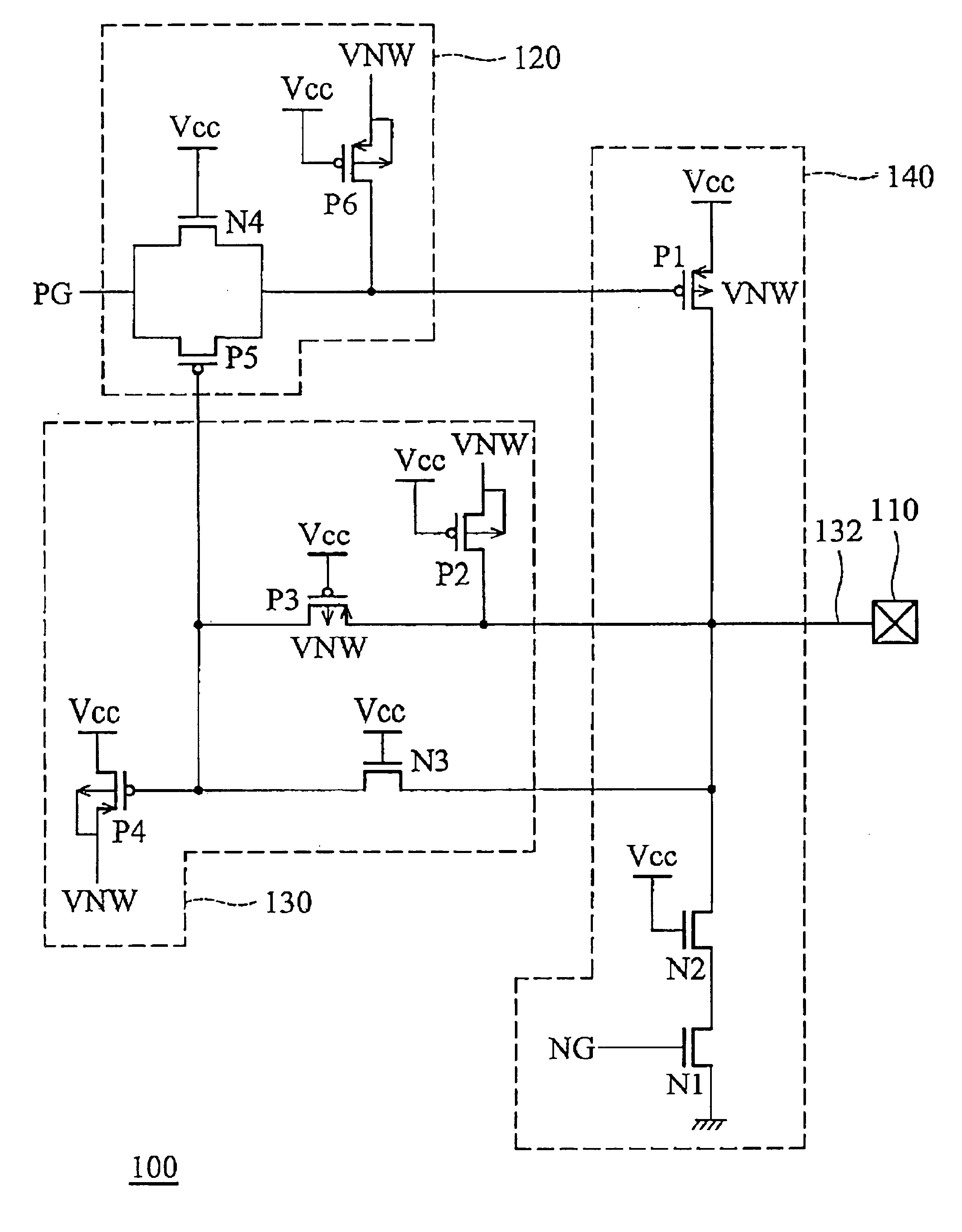
FIG. 3 is a schematic diagram showing the circuit structure of the I / O buffer according to the present invention. This I / O buffer 100 is capable of accepting an input logic signal higher than the system voltage VCC. In the following embodiment of the present invention, the system voltage VCC is 3.3V, and the input logic signal switches between 0V and 5V, wherein the 5V high-voltage logic state is higher than the system voltage VCC of 3.3V. However, it is to be understood that the invention is not limited to this embodiment.
As shown in FIG. 3, the I / O buffer 100 has an I / O circuit 140, a P-gate control circuit 120 and a N-well control circuit 130. The I / O buffer 100 is connected to an I / O pad 110 of the IC device (not shown) through an I / O port 132. The operating of the I / O buffer 100 is controlled by two gate control signals PG and NG from the core circuit (not shown).
In this embodiment, the I / O circuit 140 is composed of a PMOS transistor P1 and two NMOS transistors N1 and N2. In t...
PUM
 Abstract
Description
Claims
Application Information
 - R&D
- Intellectual Property
- Life Sciences
- Materials
- Tech Scout
- Unparalleled Data Quality
- Higher Quality Content
- 60% Fewer Hallucinations
Browse by: Latest US Patents, China's latest patents, Technical Efficacy Thesaurus, Application Domain, Technology Topic, Popular Technical Reports.
© 2025 PatSnap. All rights reserved.Legal|Privacy policy|Modern Slavery Act Transparency Statement|Sitemap|About US| Contact US: help@patsnap.com


