Insulated gate type semiconductor device and method for fabricating the same
- Summary
- Abstract
- Description
- Claims
- Application Information
AI Technical Summary
Benefits of technology
Problems solved by technology
Method used
Image

Examples
embodiment mode 1
(Embodiment Mode 1)
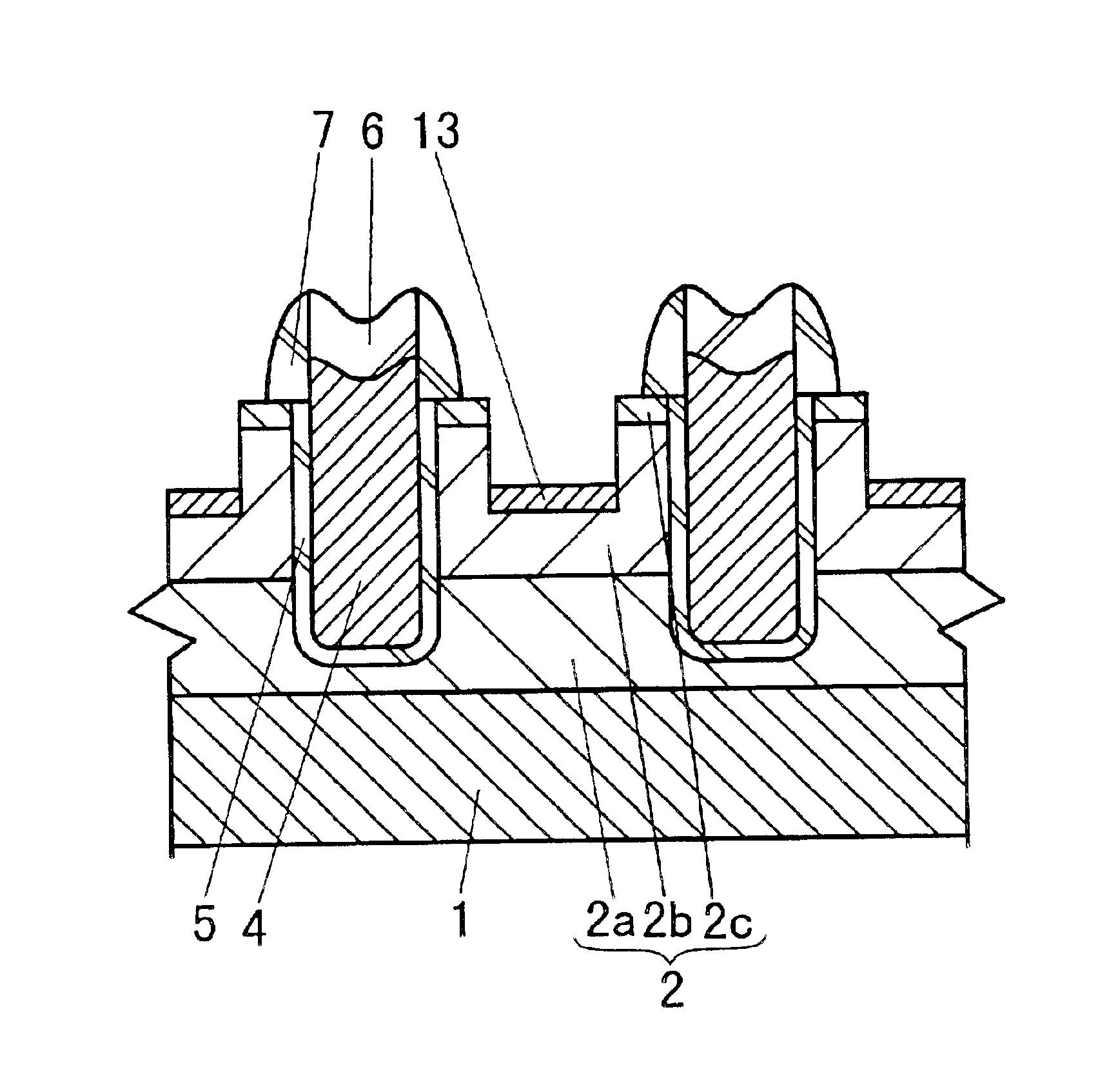
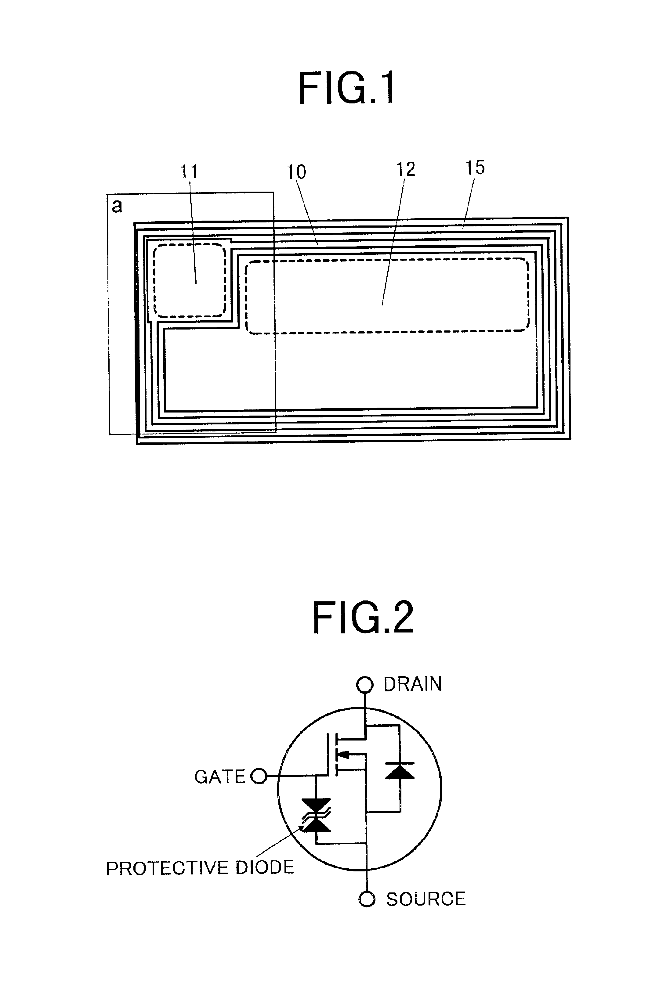
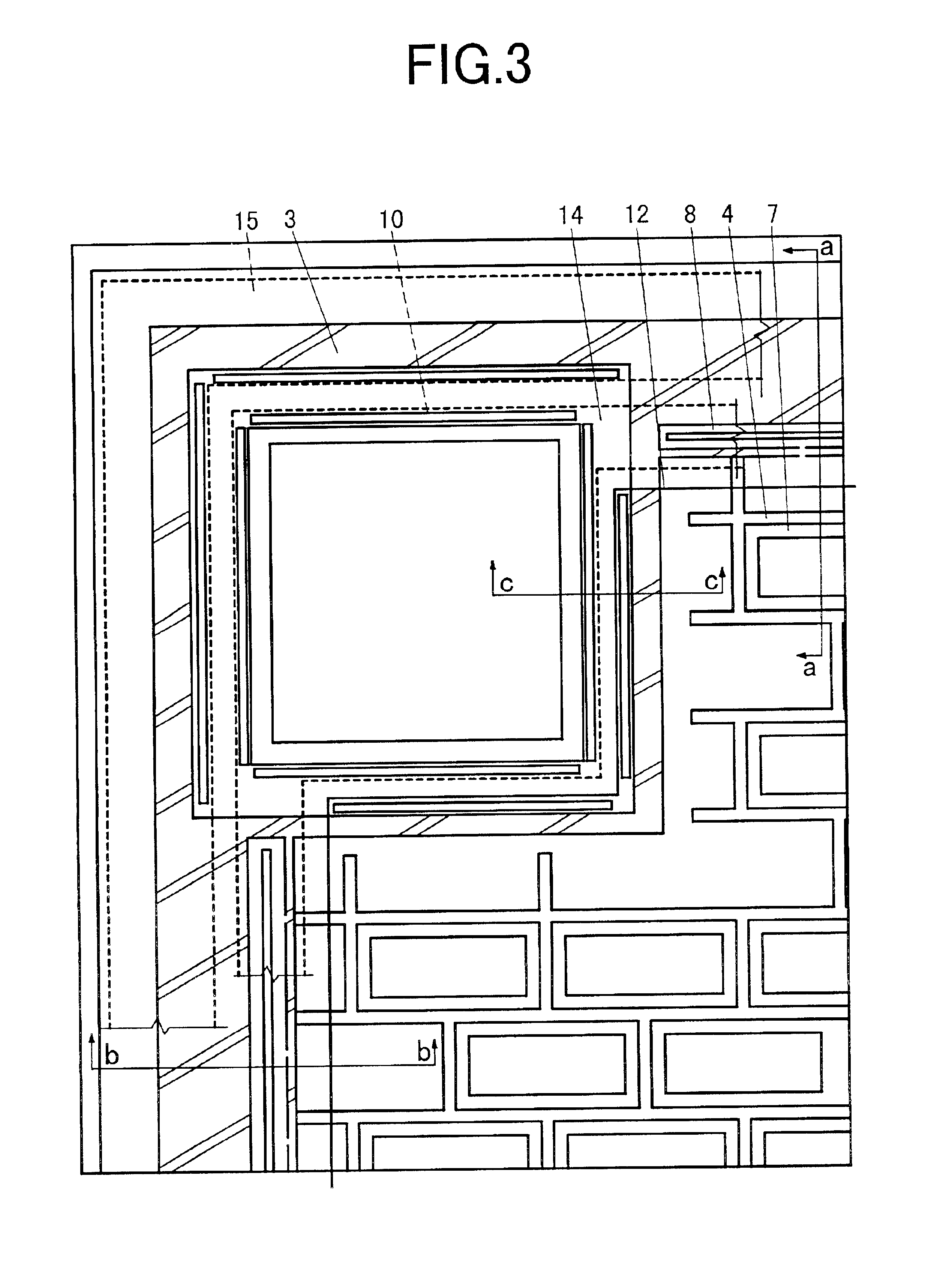
FIG. 1 is a plan view for representing a longitudinal type power MISFET having a trench-gate corresponding to a semiconductor device according to an embodiment mode 1 of the present invention. FIG. 2 is an equivalent circuit diagram for illustratively representing this power MISFET. FIG. 3 is a plan view of indicating a major portion “a” shown in FIG. 1, while this major portion “a” is enlarged. FIG. 4 is a longitudinal sectional view of the power MISFET, taken along a line “a” to “a” of FIG. 3. FIG. 5 is a longitudinal sectional diagram of the power MISFET, taken along a line “b” to “b” of FIG. 3. FIG. 6 is a longitudinal sectional diagram for representing the MISFET, taken along a line “c” to “c” of FIG. 3.
The MISFET of this embodiment mode 1 is manufactured on such a substrate that, for example, an epitaxial layer 2 is formed on an n+ type semiconductor substrate made of monocrystal silicon. This MISFET is formed within a region which is surrounded by a plate-s...
embodiment mode 2
(Embodiment Mode 2)
A semiconductor manufacturing method according to an embodiment mode 2 of the present invention owns only such a different technical method from that of the above-described embodiment mode 1, namely a method of forming a cap insulating film 6. However, other manufacturing methods of this embodiment mode 2 are substratially identical to those of the embodiment mode 1.
The method for manufacturing the semiconductor device according to the embodiment mode 2 will now be explained with reference to FIG. 7 to FIG. 10, and FIG. 17 to FIG. 20.
First, as indicated in FIG. 7, an insulating film 19 having a relatively thick thickness and made of a silicon oxide film having a thickness of 900 nm is formed on a major surface of a semiconductor substrate. A resist mask 20 is formed by way of the photolithography on the insulating film 19 within a cell forming region which is surrounded by a field insulating film 3. This resist mask 20 opens a pattern of a gate conductive layer 4 ...
embodiment mode 3
(Embodiment Mode 3)
FIG. 21 is a longitudinal sectional view for indicating a modification of the above-explained gate pillar structure in the embodiment mode 1. In this modified gate pillar structure, an upper end of a gate conductive layer 4 is located lower than a major surface of a semiconductor substrate, but a portion of a cap insulating film 6 is made higher than the major surface of the semiconductor substrate. Structures of this semiconductor device other than this modified gate pillar structure are similar to those shown in the embodiment mode 1.
In accordance with the structure of this embodiment mode 3, since a thickness of the cap insulation film 6 is made thick, electric insulating characteristics between the gate and the source can be sufficiently secured. It should also be understood that a specific care should be taken to the following aspect. That is to say, the gate conductive layer 4 made in contact with the gate insulating film 5 is not brought into the offset sta...
PUM
 Abstract
Description
Claims
Application Information
 - R&D
- Intellectual Property
- Life Sciences
- Materials
- Tech Scout
- Unparalleled Data Quality
- Higher Quality Content
- 60% Fewer Hallucinations
Browse by: Latest US Patents, China's latest patents, Technical Efficacy Thesaurus, Application Domain, Technology Topic, Popular Technical Reports.
© 2025 PatSnap. All rights reserved.Legal|Privacy policy|Modern Slavery Act Transparency Statement|Sitemap|About US| Contact US: help@patsnap.com