Non-volatile memory device with burst mode reading and corresponding reading method

a non-volatile memory and burst mode technology, applied in the field of non-volatile memories, can solve the problems of limited burst mode reading in flash memory and mode permitted

Inactive Publication Date: 2005-02-08
MICRON TECH INC
View PDF9 Cites 9 Cited by
  • Summary
  • Abstract
  • Description
  • Claims
  • Application Information

AI Technical Summary

Benefits of technology

[0015]The concept of the present invention is to automatically activate the burst read mode after a first random reading, and reading in parallel a number of words internally of the memory once a first reading is performed in the random mode, which would therefor

Problems solved by technology

However, burst reading in Flash memories is limited by the number of successive words at the predetermined starting address.
T

Method used


Image

  • Non-volatile memory device with burst mode reading and corresponding reading method
  • Non-volatile memory device with burst mode reading and corresponding reading method
  • Non-volatile memory device with burst mode reading and corresponding reading method

Examples


Embodiment Construction

volatile memory device according to the present invention.

[0022]FIG. 3 graphically illustrates control signals plotted against the same time base as they appear in a memory device equipped with the read circuit according to the present invention.

[0023]FIG. 4 illustrates a detailed block diagram of the read circuit illustrated in FIG. 2.

[0024]FIG. 5 graphically illustrates control signals plotted against the same time base as they appear in FIG. 4.

DETAILED DESCRIPTION OF THE PREFERRED EMBODIMENTS

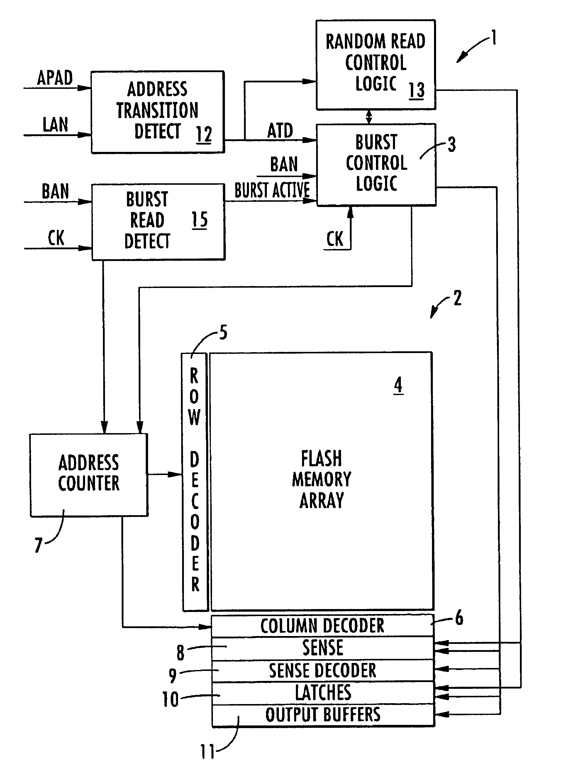
[0025]Referring to the drawing figures, and in particular to FIG. 2, a portion of a read circuit according to the present invention for a semiconductor integrated non-volatile memory device 2 is generally shown at 1 in schematic form. The memory 2 is connected to a microprocessor or a microcontroller, and can even be a type of memory integrated with the microprocessor in a single integrated circuit chip.

[0026]The construction of the read circuit portion 1 will now be described. A specific bur...


PUM


Abstract

A read control circuit and a reading method for an electronic memory device integrated on a semiconductor includes a non-volatile memory matrix with associated row and column decoders connected to respective outputs of an address counter. An address transition detect (ATD) circuit detects an input transition as the memory device is being accessed, and read amplifiers and attendant registers transfer the data read from the memory matrix to the output. The read control circuit includes a detection circuit to which is input a clock signal and a logic signal to enable reading in the burst mode. A burst read mode control logic circuit is connected downstream of the detection circuit. The method includes accessing the memory matrix in a random read mode, detecting a request for access in the burst read mode, and executing the parallel reading of a plurality of memory words during a single period of time clocked by the clock signal.

Description

FIELD OF THE INVENTION[0002]The present invention relates to non-volatile memories, and specifically concerns a memory of the flash EEPROM type. More particularly, the invention relates to a read control circuit for an electronic memory device integrated on a semiconductor, and includes a non-volatile memory matrix with associated row and column decoders which are connected to respective outputs of an address counter. An address transition detect (ATD) circuit detects an input transaction as the memory device is being accessed, and read amplifiers and associated registers transfer the data read from the memory to the output. The invention also relates to a method of reading data contained in an integrated non-volatile memory device.BACKGROUND OF THE INVENTION[0003]Current microprocessors and microcontrollers require input data at ever faster rates which exceed the limits of conventional memory technologies. Manufacturers of semiconductor memory devices are developing progressively f...

Claims


Application Information

Patent Timeline
IPC IPC(8): G11C7/10
CPCG11C7/1033G11C7/1072G11C7/1045
Inventor BARTOLI, SIMONEGERACI, ANTONINOSALI, MAUROBEDARIDA, LORENZO
Owner MICRON TECH INC
Why Eureka
Try Eureka