
Epitaxial CoSi2 on MOS devices

a technology of mos and cosi, applied in the direction of crystal growth process, polycrystalline material growth, chemically reactive gases, etc., can solve the problem of abnormal junction current, especially severe current leakage, and the non-uniform interface between polycrystalline cosisub>2 /sub>and si, so as to prevent excessive “over-etching” in the formation of electrical contacts on the mos device.

Inactive Publication Date: 2005-01-25
THE BOARD OF TRUSTEES OF THE UNIV OF ILLINOIS
View PDF7 Cites 5 Cited by
  • Summary
  • Abstract
  • Description
  • Claims
  • Application Information

AI Technical Summary

Problems solved by technology

One problem associated with this technique is that the resultant non-uniform silicide-silicon interface could cause abnormal junction leakage current, especially in deep sub-micron devices equipped with shallow junctions.
Specifically, the non-uniform interface between polycrystalline CoSi2 and Si creates localized weak-spots.
Current leakage can be especially severe if the depth of the junction is shallow, e.g., as in deep sub-micron devices.
In these processes, excessive loss of CoSi2 during contact etching processes could result in high contact resistance and degrade the device performance and reliability.
A drawback associated with any additional layer, though, is the addition of a step in the device manufacturing process, which increases manufacturing costs.
There is also a likelihood of device damage as a result of PID (plasma induced damage) damage during the PECVD deposition process.
Also, the presence of the additional layer of silicon nitride reduces the spacing between the adjacent polysilicon electrodes, and therefore poses difficulty for subsequent inter-layer-dielectric (ILD) formation.

Method used


Image

  • Epitaxial CoSi2 on MOS devices
  • Epitaxial CoSi2 on MOS devices
  • Epitaxial CoSi2 on MOS devices

Examples


Embodiment Construction

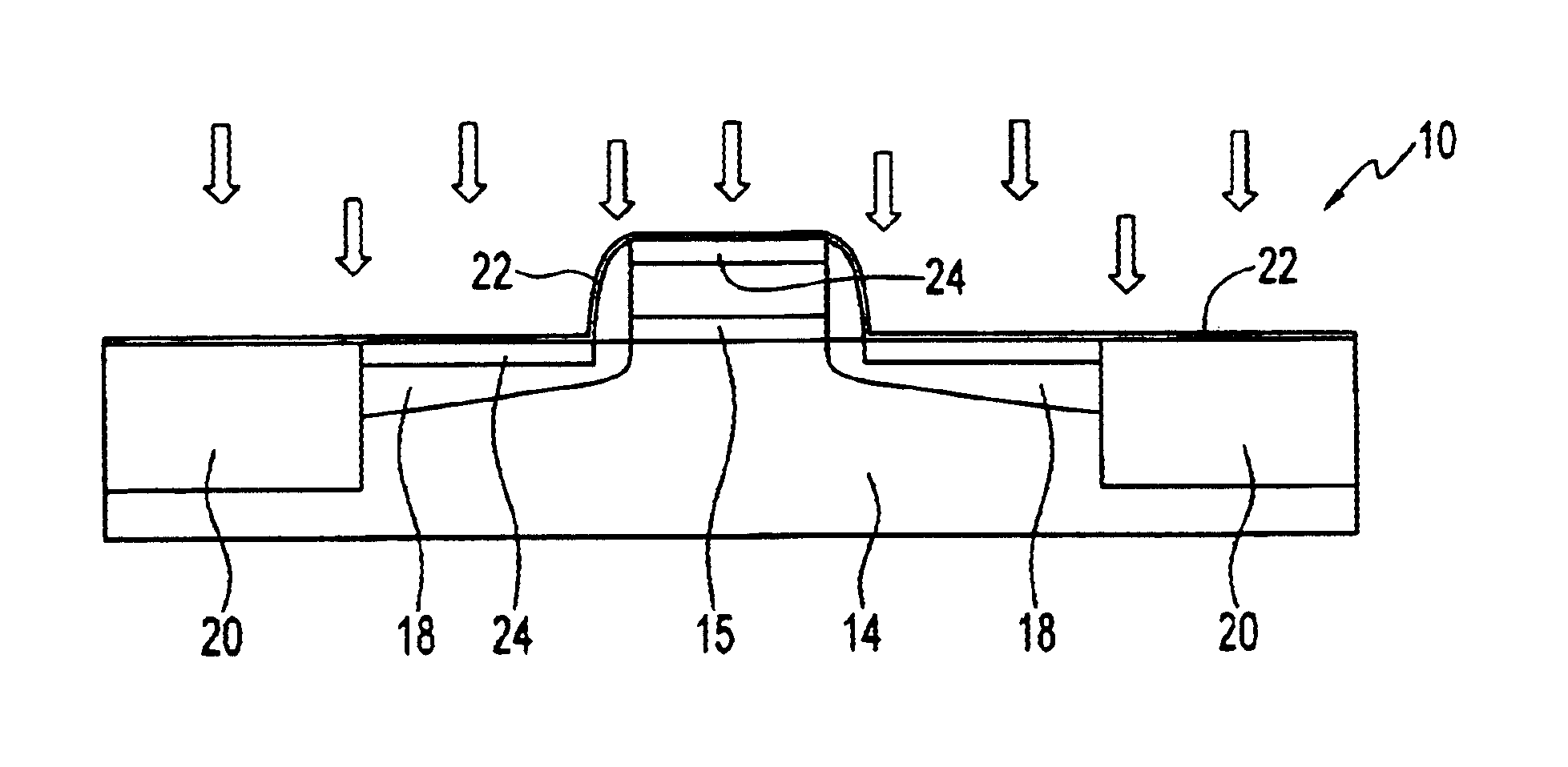
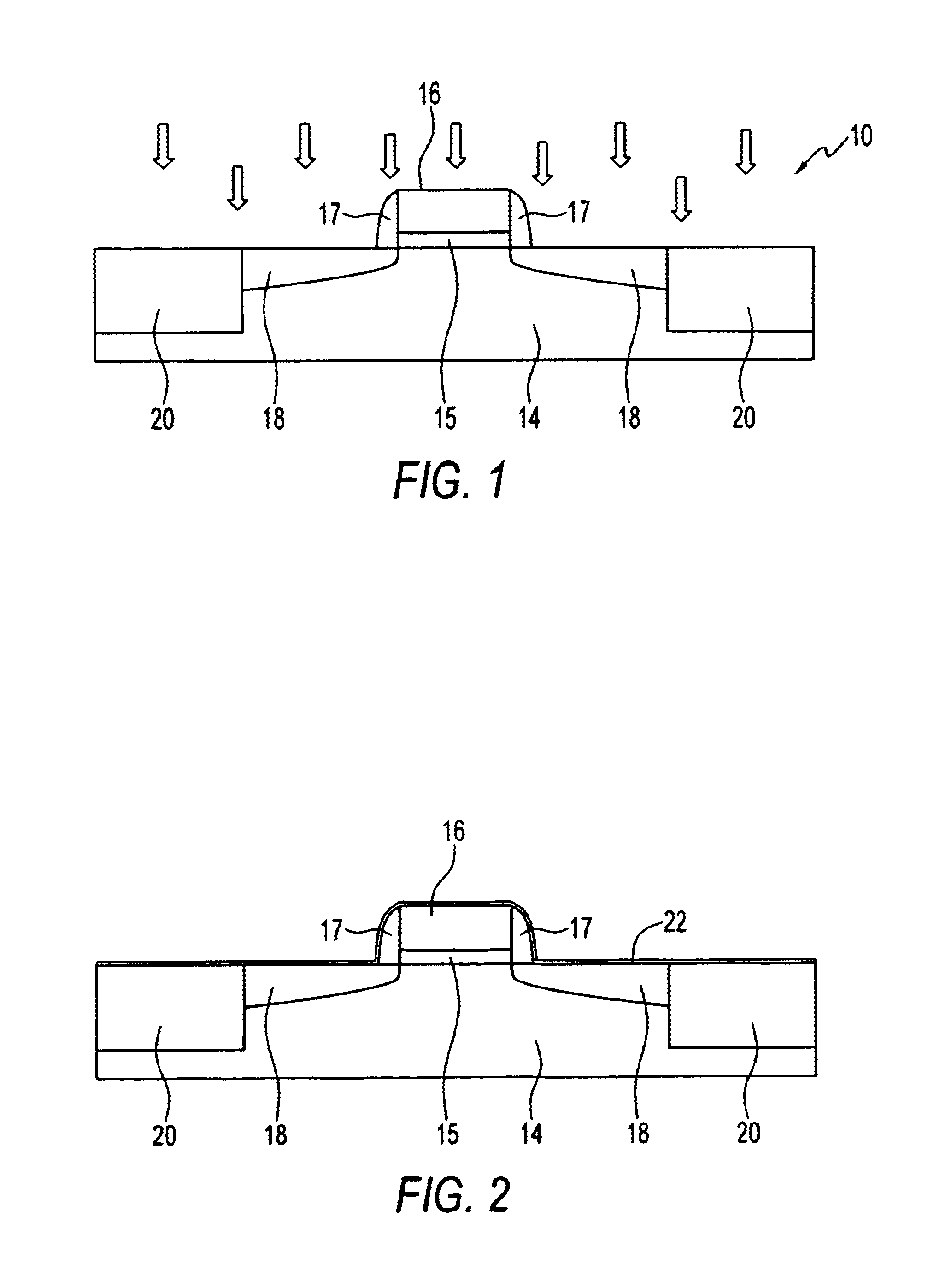
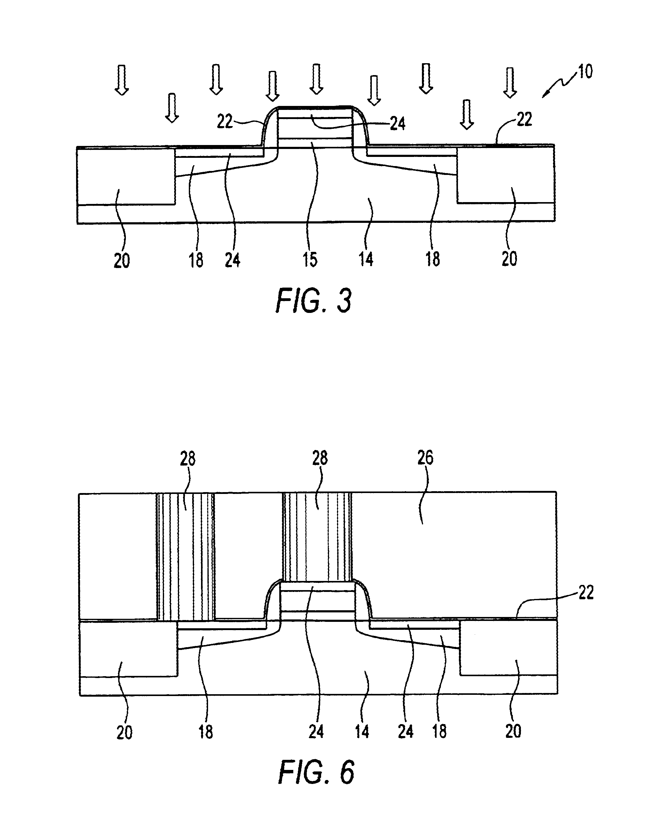
The inventors concluded that a method to form high quality epitaxial CoSi2 was needed. The invention generally concerns novel methods for formation of epitaxial CoSi2 layers on MOS devices. Methods of the invention may be used to accomplish the formation of borderless and self-aligned contacts. Borderless contacts are defined as contacts with zero or negative overlay at the border of active source / drain junctions and field-edge isolations. Self-aligned contacts are defined as contacts that are formed between two neighboring polysilicon gate electrodes, and with zero or negative overlay at the border of active source / drain junctions and spacer-isolation. Methods of the invention prevent excessive shallow trench isolation oxide gouging and silicide loss during the formation of borderless and self-aligned contacts. The use of borderless and self-aligned contacts with the invention offers the advantage of further reduction in the device's dimension. The invention will now be illustrated...


PUM

PropertyMeasurementUnit
temperatureaaaaaaaaaa
thermalaaaaaaaaaa
electrical resistanceaaaaaaaaaa

Abstract

An SixNy or SiOxNy liner is formed on a MOS device. Cobalt is then deposited and reacts to form an epitaxial CoSi2 layer underneath the liner. The CoSi2 layer may be formed through a solid phase epitaxy or reactive deposition epitaxy salicide process. In addition to high quality epitaxial CoSi2 layers, the liner formed during the invention can protect device portions during etching processes used to form device contacts. The liner can act as an etch stop layer to prevent excessive removal of the shallow trench isolation, and protect against excessive loss of the CoSi2 layer.

Description

FIELD OF INVENTIONThe field of the invention is semiconductor MOS devices. The invention particularly concerns deep sub-micron devices.BACKGROUNDCobalt silicide (CoSi2) has been widely utilized in MOS devices for electrical contacts and interconnect material. CoSi2 reduces device parasitic electrical resistance, and therefore enhances drive-current and performance of the devices. As device scaling extends into the deep sub-micron regime, shallow source / drain junctions are important to prevent junction “punch-through” and reduce the effect of drain-induced barrier lowering (DIBL).One method for fabricating a CoSi2 layer involves using polycrystalline CoSi2 film through conventional solid phase epitaxial growth. One problem associated with this technique is that the resultant non-uniform silicide-silicon interface could cause abnormal junction leakage current, especially in deep sub-micron devices equipped with shallow junctions. Specifically, the non-uniform interface between polycry...

Claims


Application Information

Patent Timeline
Patent Type & Authority Patents(United States)
IPC IPC(8): C30B1/00C30B25/02
CPCC30B1/00C30B25/02C30B29/10
Inventor LIM, CHONG WEESHIN, CHAN SOOPETROV, IVAN GEORGIEVGREENE, JOSEPH E.
Owner THE BOARD OF TRUSTEES OF THE UNIV OF ILLINOIS
Learn More