Electric double layer capacitor and method for preparing the same
a double-layer capacitor and electric double-layer technology, applied in the direction of multiple hybrid/edl capacitors, electrolytic capacitors, coatings, etc., can solve the limitations of electric double-layer capacitor miniaturization, poor mechanical strength in fusion-bonding step, and limit in size and mechanical strength which are attributed, so as to achieve high productivity of electric double-layer capacitors
- Summary
- Abstract
- Description
- Claims
- Application Information
AI Technical Summary
Benefits of technology
Problems solved by technology
Method used
Image
Examples
example 1
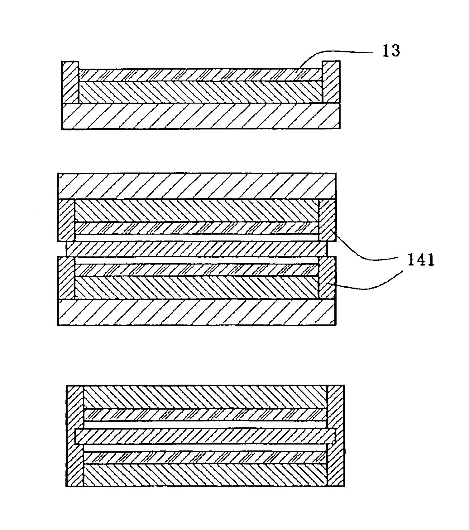
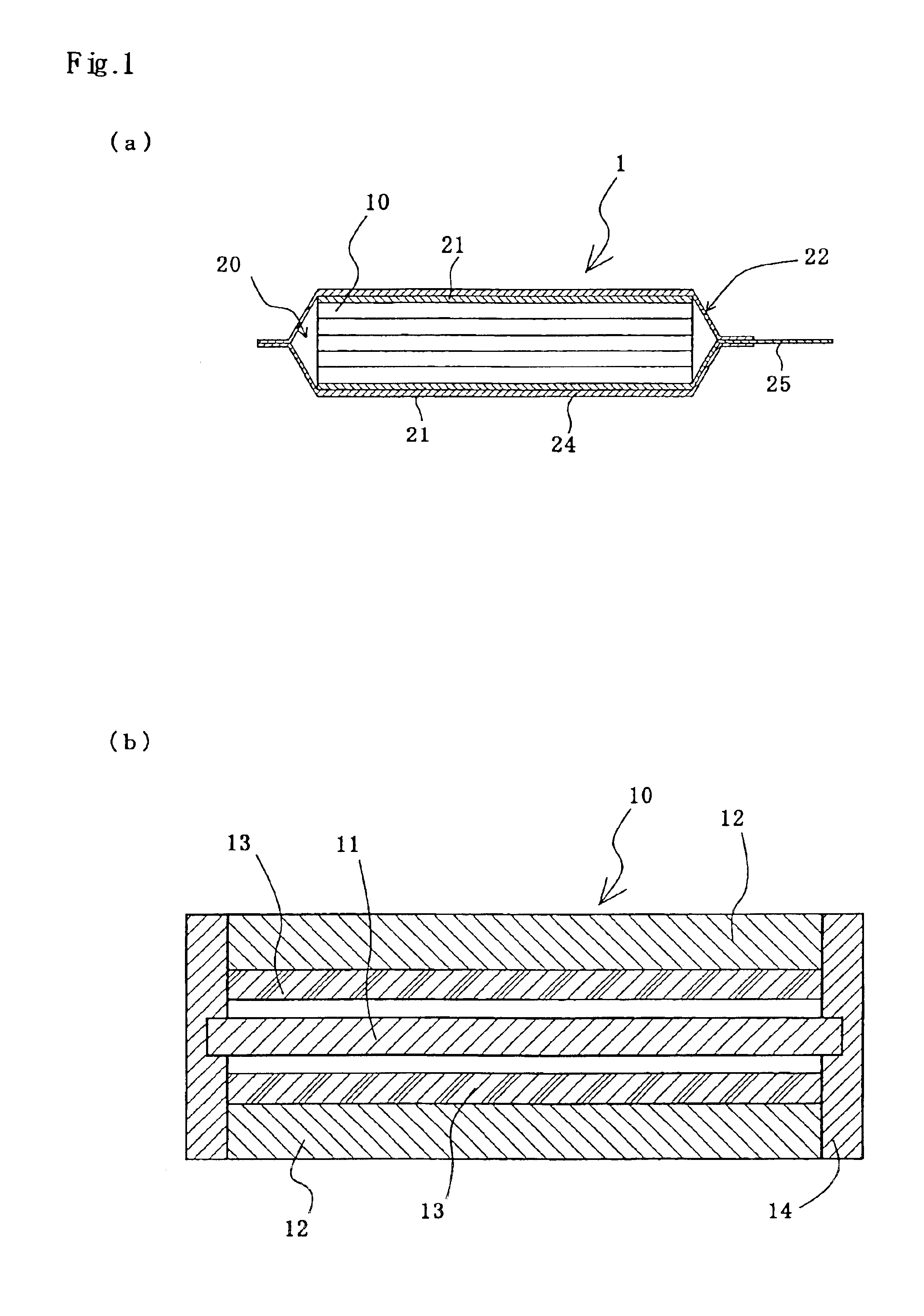
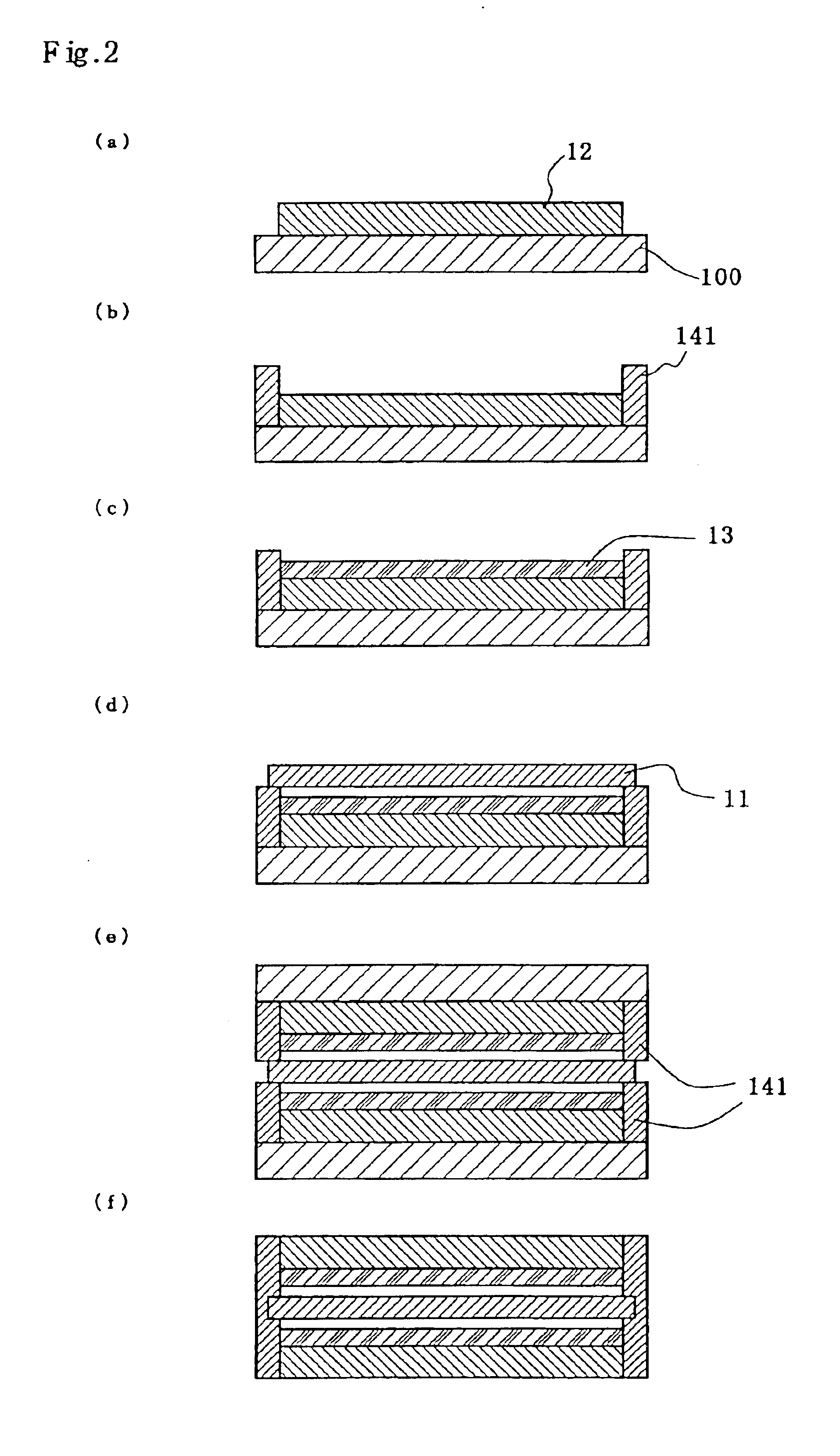
A current collector in the form of a thin film was bonded to a surface of a substrate in the form of a thin film which had a surface area larger than that of the current collector with a release agent interposed therebetween in such a manner that an uncovered marginal portion of the surface of the substrate was formed around the current collector (when viewed in plan) and that the uncovered marginal portion had such a shape as to allow a gasket element which will be described below to be disposed thereon. The current collector in the form of a thin film was made of a styrene-ethylene-butylene-styrene copolymer resin as disclosed in PCT / JP98 / 01021 and had a size of 3 cm×3 cm and a thickness of 80 μm. The substrate in the form of a thin film had a thickness of 100 μm and was made of a PET having a vapor transmission rate of 10 mg / m2 / 24 h or lower (amount of transmitted vapor is 10 mg or smaller in 24 hours per m2) measured in accordance with JIS Z 0208 test method with respect to dilu...
example 2
A sheet of thin film for current collectors was bonded to a surface of a substrate in the form of a sheet of thin film which had a surface area substantially the same as that of the sheet of thin film for current collectors with a release agent interposed therebetween. The sheet of thin film for current collectors was made of a styrene-ethylene-butylene-styrene copolymer resin as disclosed in PCT / JP98 / 01021 and had a thickness of 80 μm. The substrate in the form of a sheet of thin film had a thickness of 100 μm and was made of a PET having a vapor transmission rate of 10 mg / m2 / 24 h or lower (amount of transmitted vapor is 10 mg or smaller in 24 hours per m2) measured in accordance with JIS Z 0208 test method with respect to diluted sulfuric acid.
Then, cutting only the sheet of film for current collectors which had been applied onto the substrate, i.e., so-called “halfway cutting” was conducted to form a plurality of current collectors having a size of 3 cm×3 cm in such an arrangemen...
example 3
An electric double layer capacitor was prepared in the same manner as in Example 1 except that the gasket elements had a height of 130 μm. In this case, the value of quotient obtained by dividing the value resulting from subtraction of the thickness of the polarizable electrode from the distance between the current collector and the separator by the thickness of the separator was 0.2.
With respect to the electric double layer capacitor as obtained in this manner, ESR was 22 mΩ, and percent defective attributed to leakage of the electrolytic solution during the preparation of the electric double layer capacitor was 1.2%.
PUM
| Property | Measurement | Unit |
|---|---|---|
| distance | aaaaa | aaaaa |
| thickness | aaaaa | aaaaa |
| thickness | aaaaa | aaaaa |
Abstract
Description
Claims
Application Information
 - R&D
- Intellectual Property
- Life Sciences
- Materials
- Tech Scout
- Unparalleled Data Quality
- Higher Quality Content
- 60% Fewer Hallucinations
Browse by: Latest US Patents, China's latest patents, Technical Efficacy Thesaurus, Application Domain, Technology Topic, Popular Technical Reports.
© 2025 PatSnap. All rights reserved.Legal|Privacy policy|Modern Slavery Act Transparency Statement|Sitemap|About US| Contact US: help@patsnap.com


