Reactive formation of dielectric layers and protection of organic layers in organic semiconductor device fabrication

a technology of organic semiconductor devices and dielectric layers, which is applied in the field of reactive formation of dielectric layers and organic semiconductor device protection in organic semiconductor device fabrication, can solve the problems of ink materials, damage to organic dielectrics, and damage to organic layers or their interfaces with other layers, and achieve the effect of using damaging solvents

Inactive Publication Date: 2005-01-11
E INK CORPORATION
View PDF308 Cites 554 Cited by
  • Summary
  • Abstract
  • Description
  • Claims
  • Application Information

AI Technical Summary

Benefits of technology

The present invention provides a method to protect organic layers in OTFTs from solvent caused damage. In one embodiment, use of damaging solvents

Problems solved by technology

Unfortunately, the solvent in the ink materials will typically attack previously deposited organic layers or a polymer substrate.
This attack can lead to damage of an organic layer or its interface with other layers, as through intermixing of layers.
Solvent used to pattern the semiconductor can damage an organic dielectric, while

Method used


Image

  • Reactive formation of dielectric layers and protection of organic layers in organic semiconductor device fabrication
  • Reactive formation of dielectric layers and protection of organic layers in organic semiconductor device fabrication
  • Reactive formation of dielectric layers and protection of organic layers in organic semiconductor device fabrication

Examples


Embodiment Construction

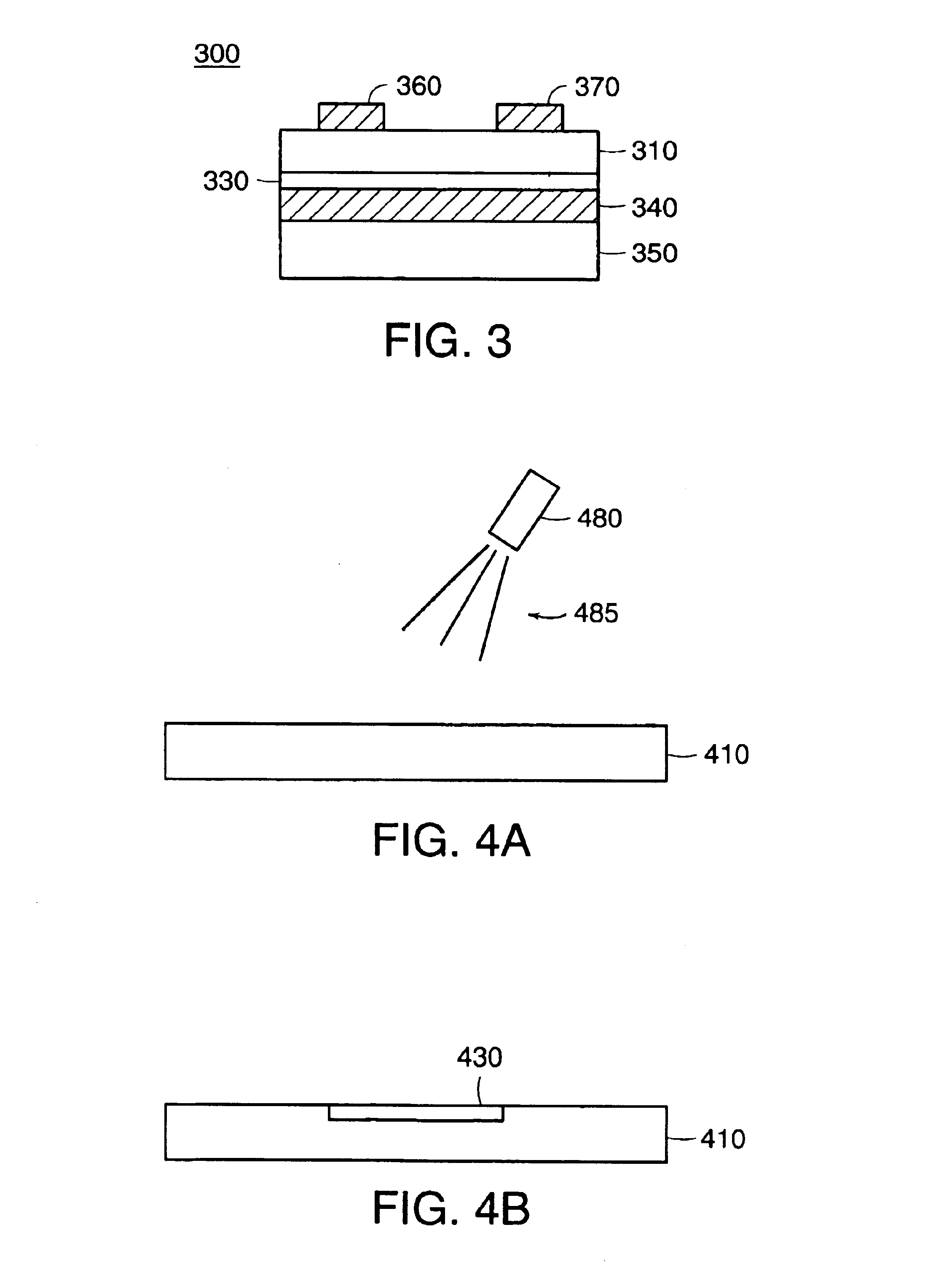
The invention relates to the manufacture of displays that utilize arrays of organic semiconductor based transistors. The invention is of particular use in the production of displays with an electrophoretic display medium and mitigates the problem of solvent attack of organic layers during manufacture. Formation of dielectric layers will first be described, followed by a description of protection of organic layers during manufacture.

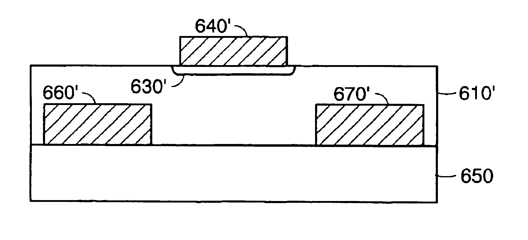
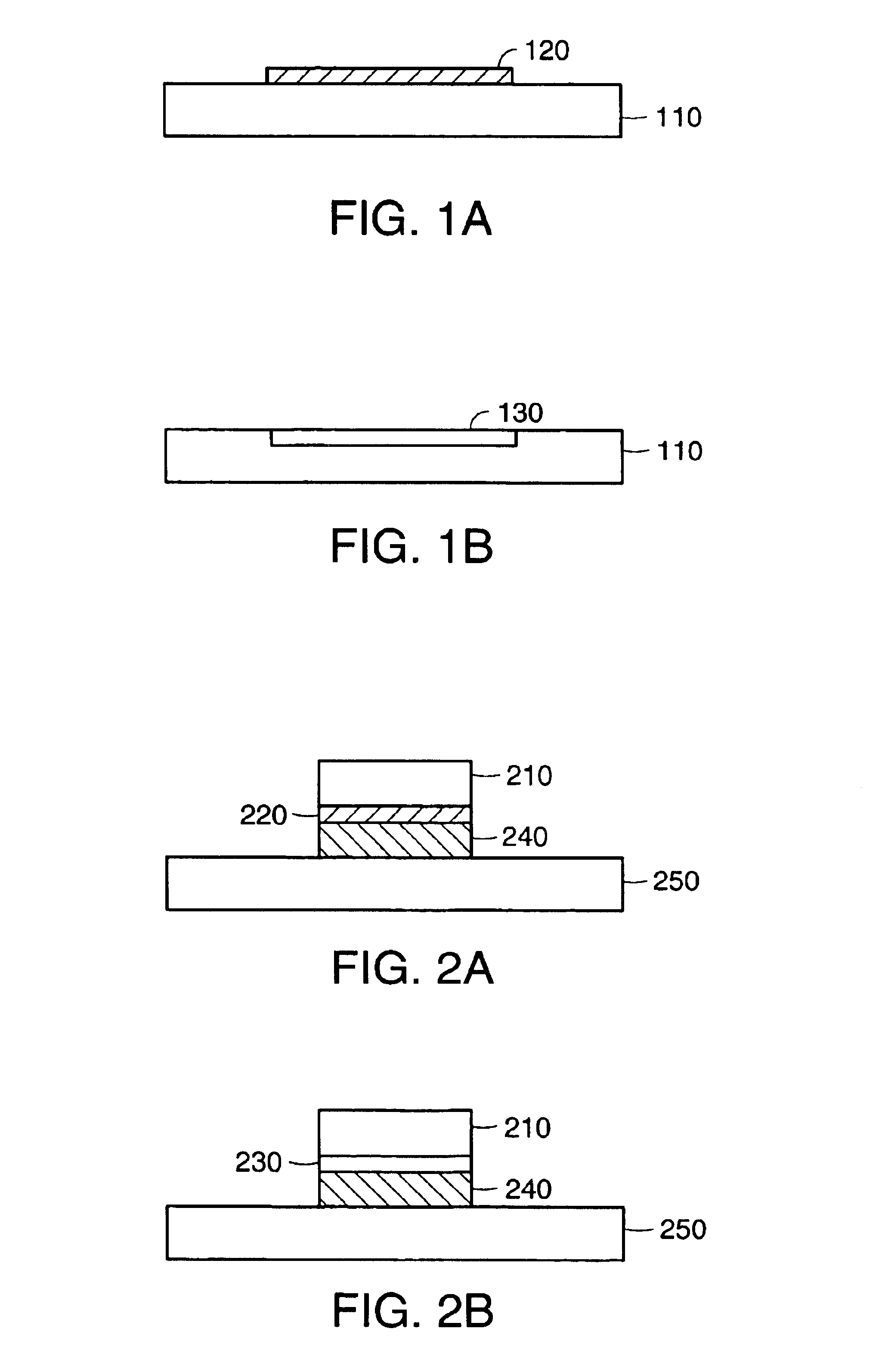
I. Method of Forming Dielectric Layers in Organic Semiconductor Devices

With reference to FIG. 1a, an embodiment is shown in which an organic semiconductor layer 110 is deposited, followed by deposition of a reactive species 120. The reactive species 120 can be deposited uniformly, or patterned onto desired areas of the organic semiconductor. The reactive species 120 is selected from a variety of materials that are reactive with the organic semiconductor. The selected material will depend on the type of desired reaction, for example, reduction, oxidation, ...


PUM

PropertyMeasurementUnit
Dielectric polarization enthalpyaaaaaaaaaa

Abstract

In one embodiment of the invention, a method of manufacturing a semiconductor device comprises the steps of: a) providing an organic semiconductor layer; b) depositing a reactive species on a portion of the organic semiconductor layer; and c) reacting the reactive species with the portion of the organic layer to form a dielectric layer.

Description

TECHNICAL FIELDThe invention relates generally to manufacturing of semiconductor devices and more particularly the protection during manufacture of organic layers in organic material-based electronic devices.BACKGROUND OF THE INVENTIONThe fabrication of all-printed backplanes on polymeric substrates through use of solvent-based inks offers the potential for lower cost, flexible, or large area displays. There are numerous potential applications for such displays, such as: rolled displays; affordable large area displays; displays incorporated into fabrics; and as a paper substitute. Unfortunately, the solvent in the ink materials will typically attack previously deposited organic layers or a polymer substrate. This attack can lead to damage of an organic layer or its interface with other layers, as through intermixing of layers.In particular, the interface between an organic semiconductor and a gate dielectric is critical to the performance of a organic-based thin-film transistor (“OT...

Claims


Application Information

Patent Timeline
IPC IPC(8): G02F1/13G02F1/1362G02F1/1345H01L51/40H01L51/05G02F1/1334H01L51/00
CPCG02F1/1345G02F1/1362H01L51/0002H01L51/0516G02F1/1334H01L51/055H01L51/0512H01L51/0541H01L51/0545H01L51/0015H10K71/10H10K71/211H10K10/468H10K10/462H10K10/481H10K10/466H10K10/464
Inventor DRZAIC, PAUL S.WANG, JIANNA
Owner E INK CORPORATION
Why Eureka
Try Eureka