Eureka AIR delivers breakthrough ideas for toughest innovation challenges, trusted by R&D personnel around the world.

Method and apparatus for forming an HSG-Si layer on a wafer

Inactive Publication Date: 2005-01-04
SAMSUNG ELECTRONICS CO LTD
View PDF24 Cites 10 Cited by
  • Summary
  • Abstract
  • Description
  • Claims
  • Application Information

AI Technical Summary

Benefits of technology

Accordingly, one object of the present invention is to provide a method of forming an HSG-Si layer in a relatively short amount of time and under a uniform temperature condition, thereby preventing defects from occurring in the HSG-Si layer and contributing to the overall efficiency and productivity of a semiconductor device manufacturing process. Another object of the present invention is to provide an apparatus of a relatively simple structure for forming an HSG-Si layer under a uniform temperature condition, thereby preventing defects from occurring in the HSG-Si layer and reducing equipment costs associated with a semiconductor device fabrication facility.
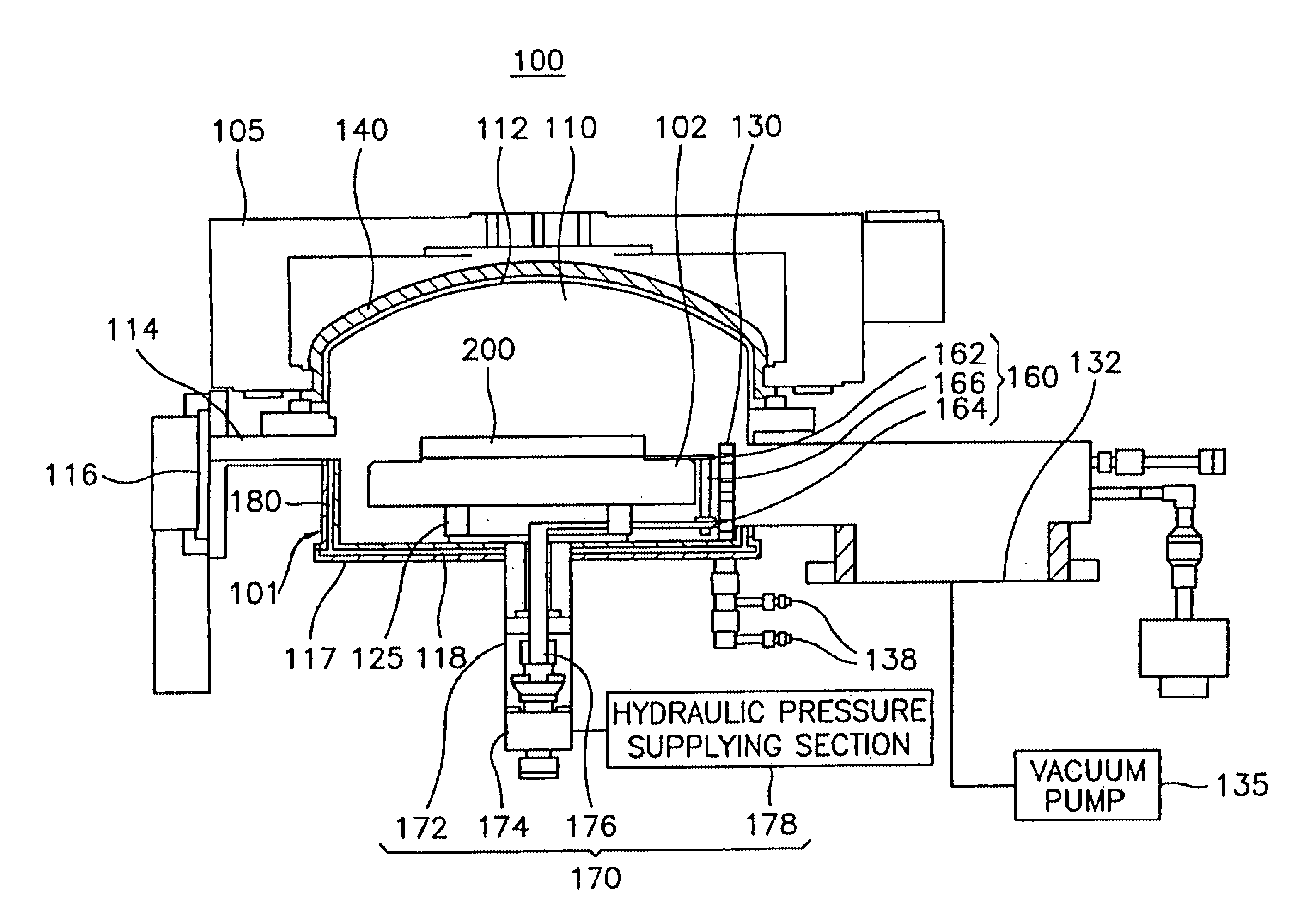
In order to achieve the second object, the present invention provides a semiconductor processing apparatus having a housing constituting a process chamber in which the HSG-Si manufacturing process is performed, a first heater fixed in place at the bottom of the process chamber, a gas injector disposed at the same level as the first heater, and a thermal insulator which insulates the process chamber to prevent the loss of heat from the process chamber.
A temperature control system allows the temperature of the first and second heaters and, hence, the temperature of the ambient within the process chamber and the surface temperature of the wafer itself, to be regulated. The temperature control system includes at least one temperature sensor, such as a thermocouple, and a current supply line attached to the first heater.

Problems solved by technology

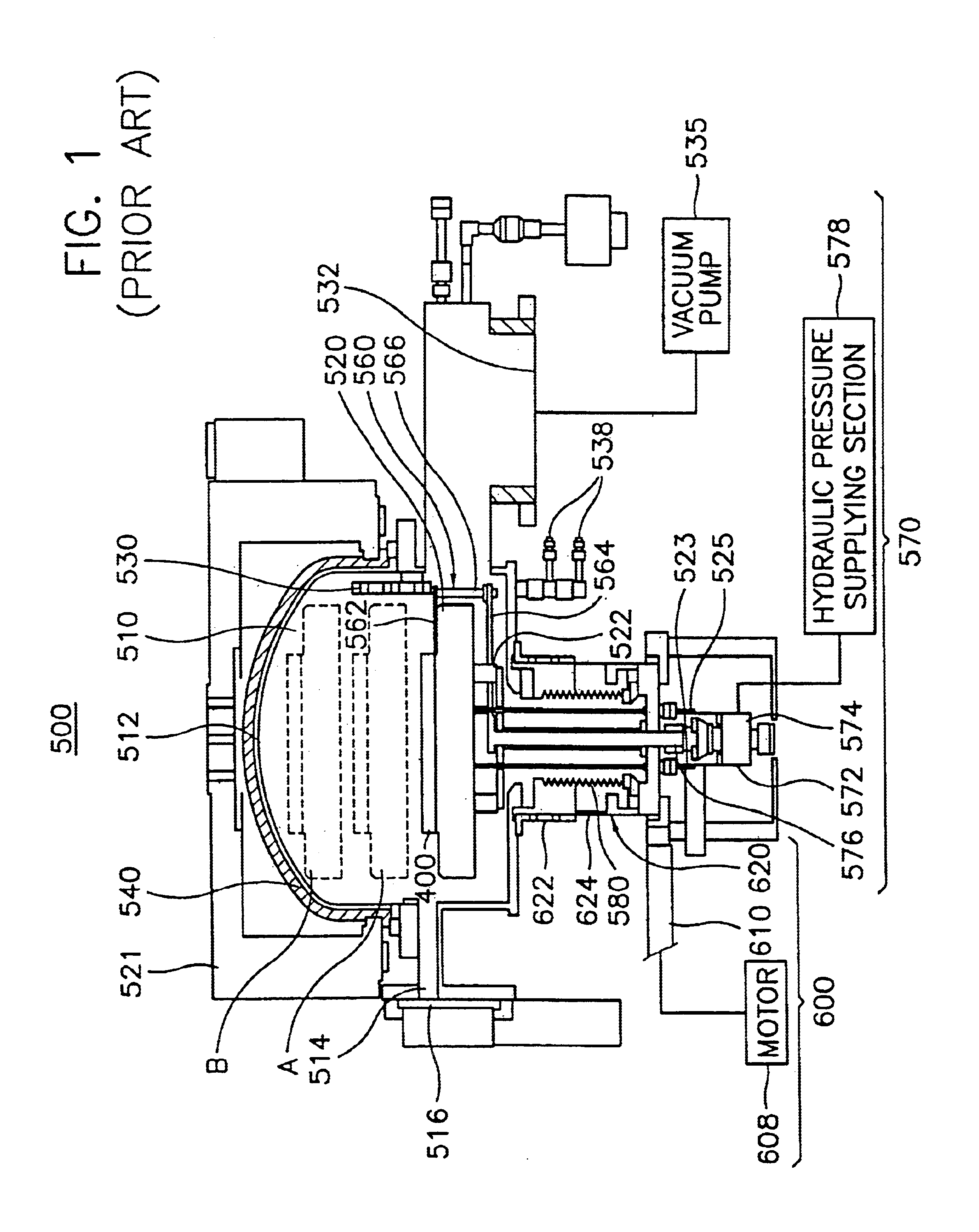
Furthermore, the heater moving apparatus 600 for moving the first heater 520 upward and downward renders the overall structure of the apparatus complex, and contributes significantly to the manufacturing cost of the apparatus.
Furthermore, moving the first heater 520 upward and downward during the forming of the HSG-Si layer takes time, thereby detracting from the productivity of the manufacturing process.

Method used


Image

  • Method and apparatus for forming an HSG-Si layer on a wafer
  • Method and apparatus for forming an HSG-Si layer on a wafer
  • Method and apparatus for forming an HSG-Si layer on a wafer

Examples


Embodiment Construction

Hereinafter, a preferred embodiment of the present invention will be explained in detail with reference to the attached drawings.

Referring to FIG. 2 an apparatus 100 for forming an HSG-Si layer on a wafer according to the present invention includes a housing 101 forming a process chamber 10 therein. The housing 101 includes a bottom wall 17 extending along the bottom of the process chamber 110.

A first heater 102 for heating a wafer 200 is fixed in place in the process chamber 110. More specifically, the bottom surface of the first heater 102 is supported by a support member 125 fixed to the bottom wall 117 of the housing 101. The wafer 200 is introduced into the process chamber 110 through a guide slot 114 formed at one side of the process chamber 110 and is positioned on the upper surface of the first heater 102.

Referring to FIG. 3, first and second thermocouples 122 and 123 for detecting temperatures of the central and peripheral portions of the first heater 102 and a current supp...


PUM

PropertyMeasurementUnit
Temperatureaaaaaaaaaa
Surface temperatureaaaaaaaaaa

Abstract

An HSG-Si layer is formed on a wafer under a uniform temperature condition. An apparatus for forming the HSG-Si layer includes a housing forming a process chamber, a first heater on which the wafer is positioned fixed in place at the bottom of the process chamber, a second heater at the top of the process chamber, and a thermal insulator which prevents the heat generated by the first heater from being transferred to the outside of the process chamber. A temperature control system regulates the temperature of the heaters. A method of forming the HSG layer includes steps of placing the wafer on the first heater, using the heaters to remove moisture from the wafer, injecting a source gas of the HSG-Si toward the upper surface of the wafer to form amorphous silicon on the wafer, and annealing the wafer for a predetermined period of time to transform the amorphous silicon into an HSG-Si layer. During the steps of forming the HSG-Si layer, the temperatures of the first and second heaters are regulated to maintain the surface temperature of the wafer constant.

Description

BACKGROUND OF THE INVENTION1. Field of the InventionThe present invention relates to method and apparatus for forming an HSG-Si (hemispherical grained silicon) layer. More particularly, the present invention relates to a method and apparatus for forming an HSG-Si layer on a wafer in the manufacturing of semiconductor memory devices.2. Description of the Related ArtIn general, semiconductor devices are manufactured by coating a silicon wafer with a thin film having predetermined electrical characteristics, using a semiconductor manufacturing apparatus. The thin film is typically formed on the wafer by executing a series of semiconductor processes such as lithography, chemical and physical vapor deposition, plasma etching, HSG-Si manufacturing processes or the like. The wafer coated with the thin film is used for manufacturing semiconductor devices and chips.Among the above-mentioned semiconductor manufacturing processes, the HSG-Si manufacturing process is widely used to increase the...

Claims


Application Information

Patent Timeline
IPC IPC(8): C23C16/22C23C16/24H01L21/00C23C16/56H01L21/205H01L21/363H01L21/8242H01L27/108
CPCC23C16/24C23C16/56H01L21/67103H01L21/67017H01J37/32522H01J2237/2001H10B99/00
Inventor YUN, JONG YOUNG
Owner SAMSUNG ELECTRONICS CO LTD
Why Eureka
Eureka Blog
Learn More