Light modulator
a light modulator and light source technology, applied in the field of light modulators, can solve the problems of low refrectance, difficulty in displaying white, difficult to see images on the screen,
- Summary
- Abstract
- Description
- Claims
- Application Information
AI Technical Summary
Benefits of technology
Problems solved by technology
Method used
Image
Examples
first embodiment
In a first embodiment, an electric field is applied in a direction perpendicular to or almost perpendicular to the helical axis of a ferroelectric liquid crystal in a planer state.
first example
FIG. 1
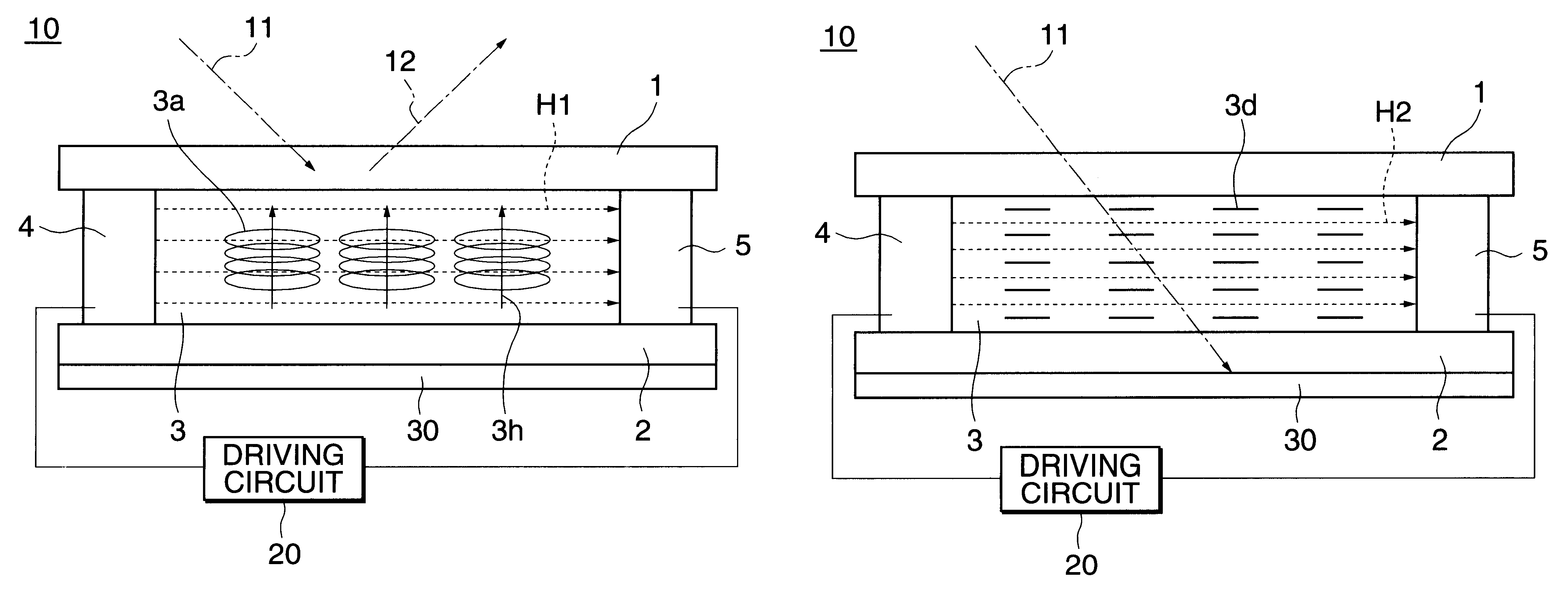
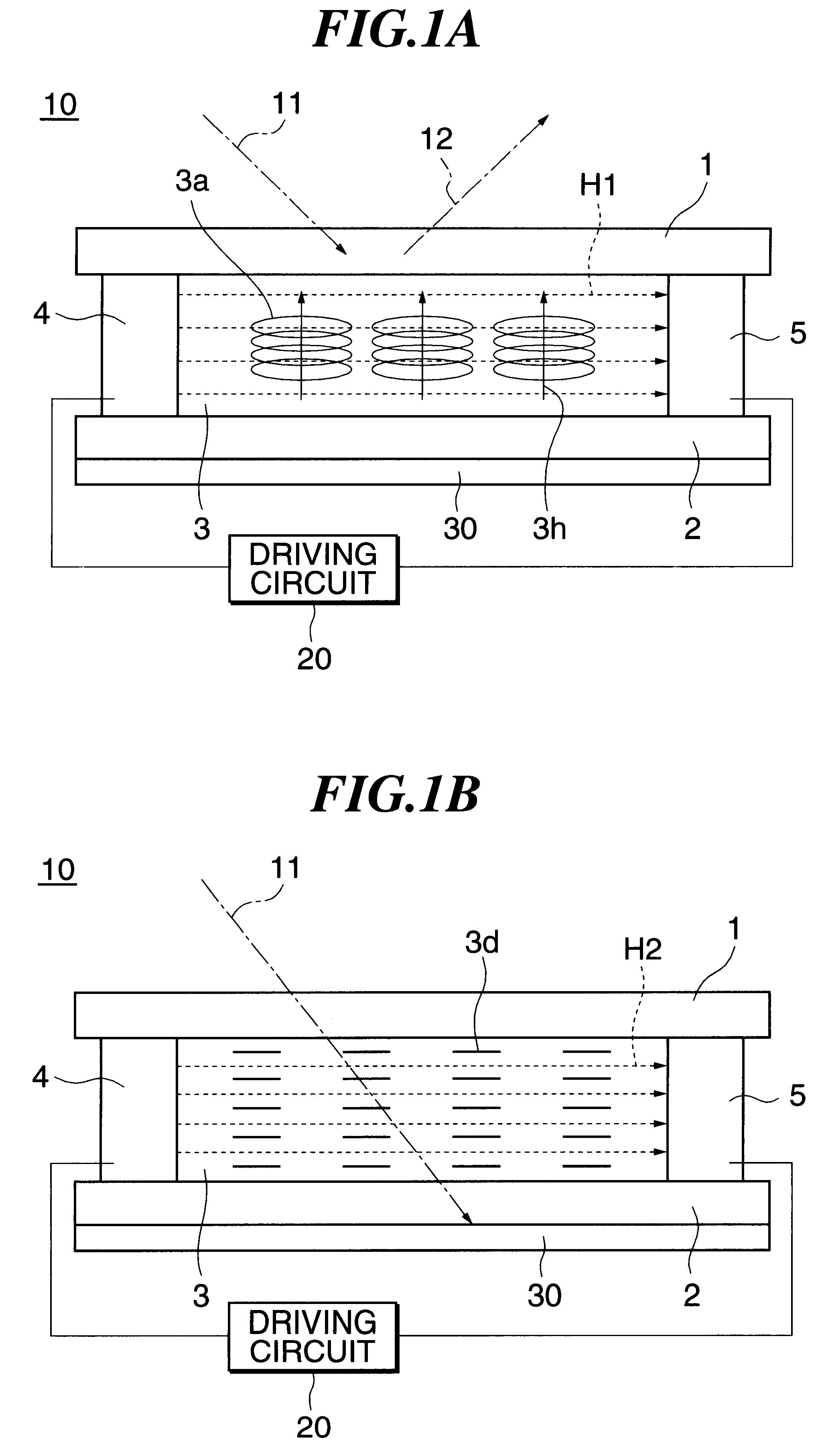
FIG. 1 shows a first example of the first embodiment.
A display device has a display element 10 and a driving circuit 20. The display element 10, in this example, has a ferroelectric liquid crystal 3 sandwiched between substrates 1 and 2, has electrodes 4 and 5 formed face to face with each other in a direction parallel to the substrates at the sides of pixels, the electrodes each interposed between the substrates 1 and 2, and has a light absorption layer (black) 30 formed on the back of the substrate 2 opposite to an observation side (a side through which outside light comes).
The substrates 1 and 2 are made of glass, plastic, or the like, wherein the substrate 1 at least at the observation side is transparent. The electrodes 4 and 5 can be made of a metal such as tantalum and chrome, and can also serve as spacers to control the gap between the substrates 1 and 2.
The ferroelectric liquid crystal 3, when no electric field is applied to it, goes into a planer state as shown in FI...
second example
FIGS. 2 to 4
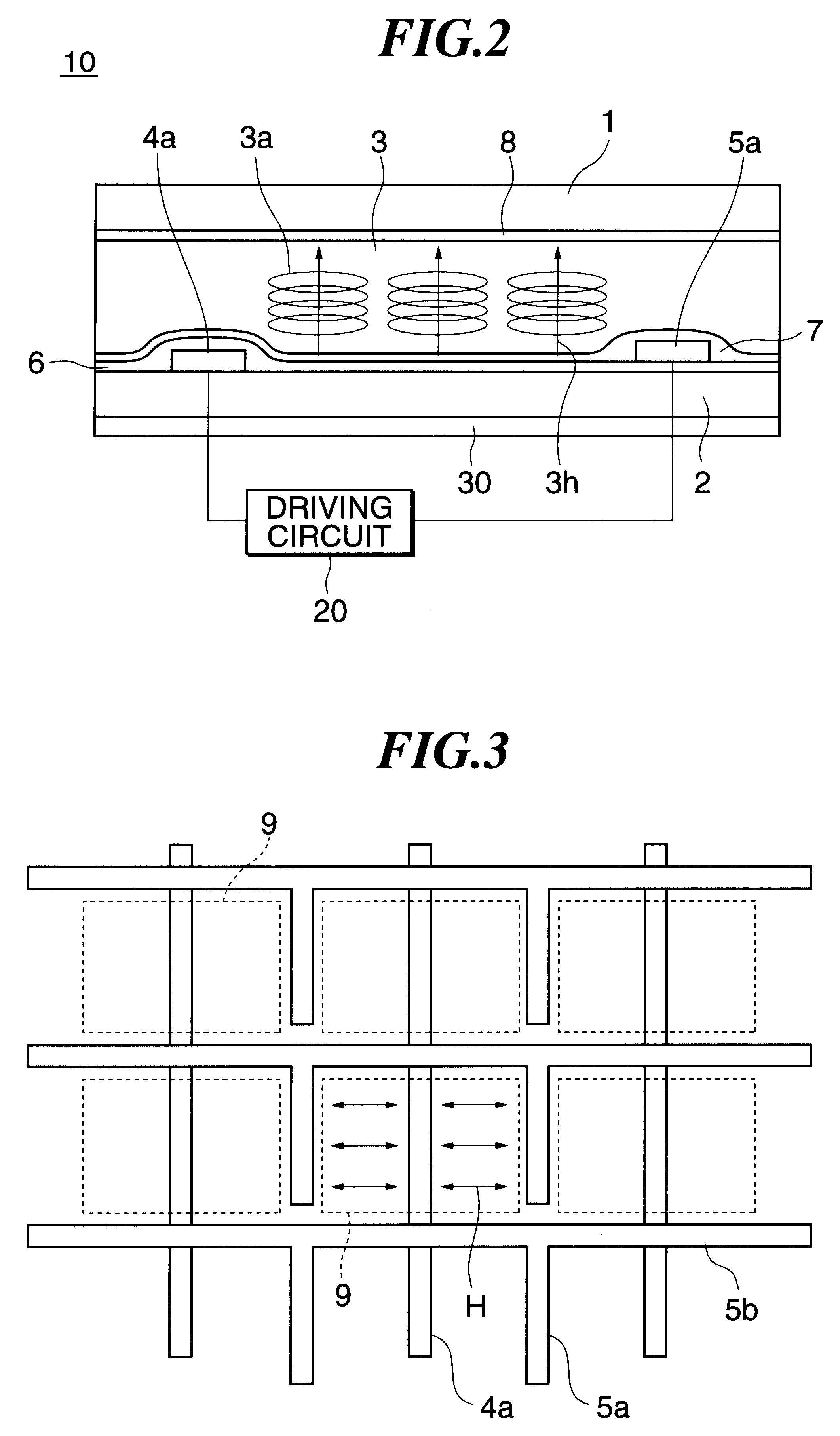
FIG. 2 shows a second example of the first embodiment.
In a display device of this example, on one substrate 2, a signal electrode 4a and a scanning electrode 5a are formed face to face with each other in a direction parallel to the substrate, and by the driving circuit 20, an electric field is applied between the electrodes 4a and 5a in a direction perpendicular to or almost perpendicular to the helical axes 3h of the ferroelectric liquid crystal 3.
Referring to FIG. 3 also, a display element of this example is described along with an example of a manufacturing method.
First, the substrate 2 is cleaned, a tantalum film 100 nm thick is produced on one surface thereof by RF sputtering, and patterning is performed in stripe shape 10 .mu.m wide by a photolithography process to form the signal electrode 4a.
Next, amorphous SiN 300 nm thick is formed on the substrate 2 containing the signal electrode 4a by plasma CVD to form an insulating layer 6.
Next, a tantalum film 100 nm thic...
PUM
| Property | Measurement | Unit |
|---|---|---|
| thick | aaaaa | aaaaa |
| thick | aaaaa | aaaaa |
| diameter | aaaaa | aaaaa |
Abstract
Description
Claims
Application Information
 - R&D
- Intellectual Property
- Life Sciences
- Materials
- Tech Scout
- Unparalleled Data Quality
- Higher Quality Content
- 60% Fewer Hallucinations
Browse by: Latest US Patents, China's latest patents, Technical Efficacy Thesaurus, Application Domain, Technology Topic, Popular Technical Reports.
© 2025 PatSnap. All rights reserved.Legal|Privacy policy|Modern Slavery Act Transparency Statement|Sitemap|About US| Contact US: help@patsnap.com


