
Method to prevent leaving residual metal in CMP process of metal interconnect

a technology of metal interconnection and residual metal, which is applied in the field of composition and removal of metal layers, can solve the problems of shorts in the semiconductor device, premature device failure, shorts in the device, etc., and achieve the effect of effectively removing metal residues

Inactive Publication Date: 2003-07-29
IBM CORP
View PDF10 Cites 16 Cited by
  • Summary
  • Abstract
  • Description
  • Claims
  • Application Information

AI Technical Summary

Benefits of technology

is to provide a CMP method which effectively removes metal residues and liner material which does away with the need for surface touch up of the dielectric.
It is yet another object of the present invention to provide an enhanced method of forming an interconnect structure which provides a substantially planar upper surface of the underlying dielectric layer.
In a second aspect, the present invention is directed to a method of polishing a semiconductor wafer comprising the steps of: providing a semiconductor wafer having an interconnect structure wherein a top surface of the wafer has a blanket layer of liner material and a blanket layer of excess metal disposed thereover; chemical mechanical polishing the wafer to remove the blanket layer of excess metal with a first slurry comprising a metal oxidizing agent while leaving a metal residue; chemical mechanical polishing the wafer to remove the metal residue with a second slurry comprising another oxidizing agent having an affinity for the excess metal and the linear material; and prevent scratching of a dielectric material beneath the liner material.

Problems solved by technology

If the process steps of device fabrication are performed on a wafer surface that is not planar, various problems can occur which may result in premature device failure.
Problems arising from this methodology involve sufficient removal of the metallization and liner material which may create isolated metal islands which can lead to shorts in the semiconductor device.
Any metal residues which remain are not removed in subsequent steps and may lead to shorts in the device.
However, the over-polishing tends to cause "dishing," erosion of the metallization within the via or interconnect, which leads to metal open defects.
Furthermore, the liner material has proven problematic in its removal, tending to remain behind in localized topography caused by prior level "dishing" and in scratches of the wafer surface.
Attempts to remove the liner material also result in surface defects of the underlying dielectric.
However, care must be taken such that the dielectric is not eroded beyond acceptable process parameters particularly in areas of high density metallization.
However, the slurry is ineffective in removing any tungsten residues which causes severe metal shorting in the resultant device.
However, any tungsten residue that remains on the wafer service will create isolated metal islands leading to shorts and premature device failure.

Method used


Image

  • Method to prevent leaving residual metal in CMP process of metal interconnect
  • Method to prevent leaving residual metal in CMP process of metal interconnect
  • Method to prevent leaving residual metal in CMP process of metal interconnect

Examples


Embodiment Construction

)

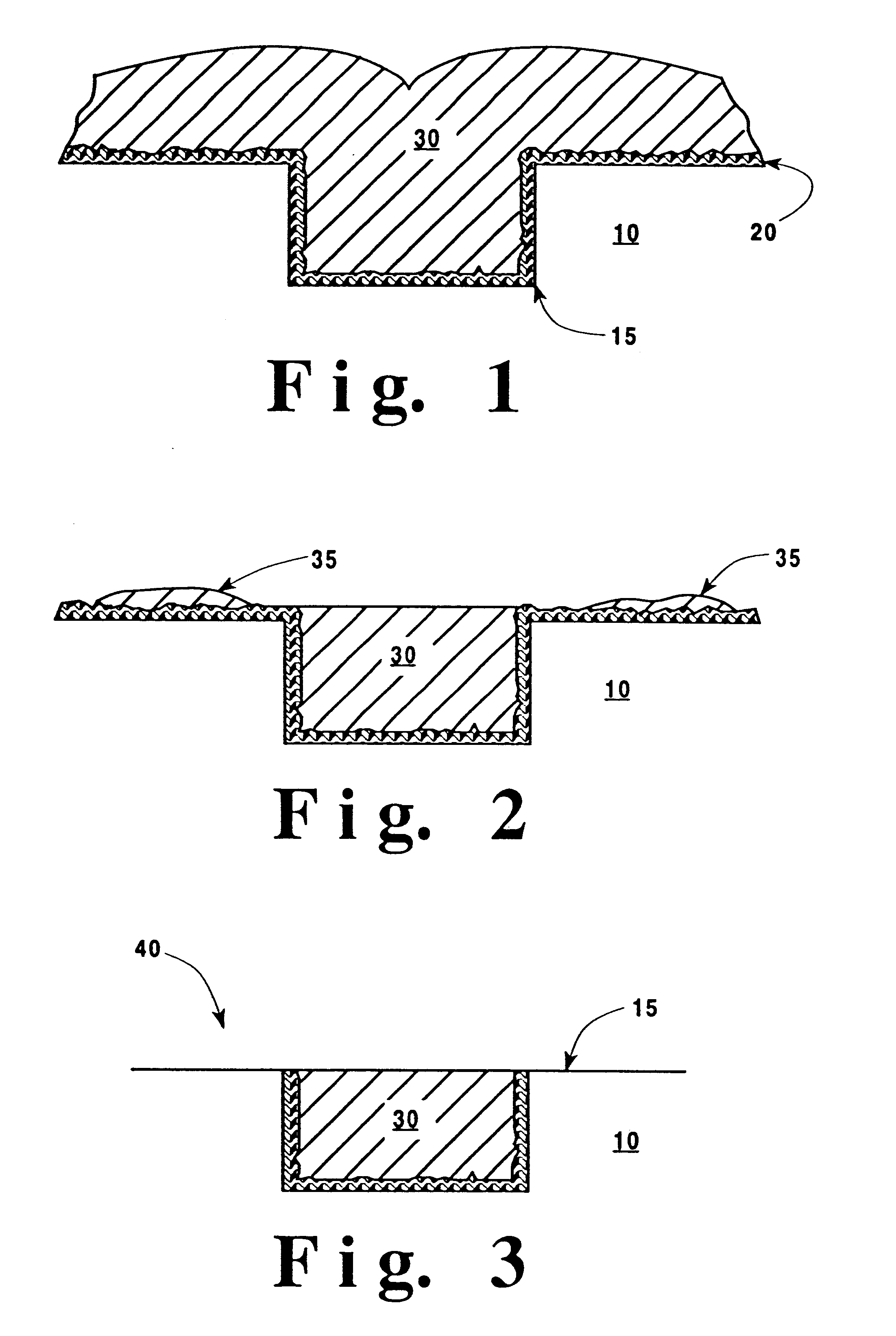
In describing the preferred embodiment of the present invention, reference will be made herein to FIGS. 1-6 of the drawings in which like numerals refer to like features of the invention. Features of the invention are not necessarily shown to scale in the drawings.

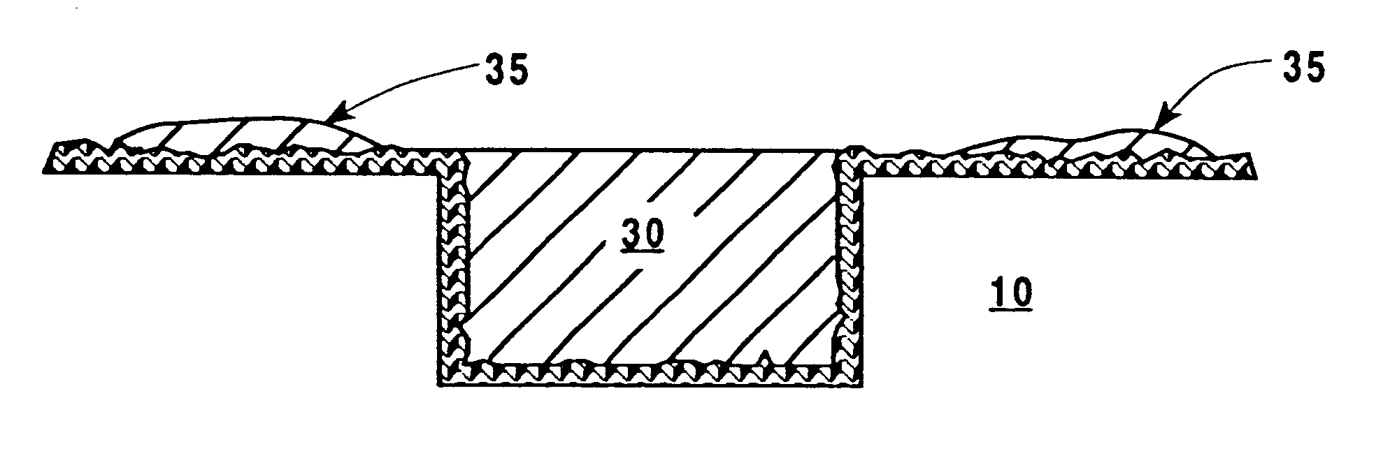
The present invention provides an enhanced CMP methodology utilizing a first slurry to planarize the metallization wherein a metal residue may remain, and a second slurry which removes the liner material. The advantage lies in that the second slurry is selective to both the liner material and any metal residue remaining. The methodology of the present invention also significantly reduces scratching of the underlying dielectric layer.

In FIG. 1 is shown a cross-sectional view of a portion of an interconnect structure having a dielectric layer 10 in which a via 15 has been etched. Dielectric layer 10 may comprise any appropriate type of insulating material known in the art such as silicon dioxide, and different types of dope...


PUM

PropertyMeasurementUnit
Dielectric polarization enthalpyaaaaaaaaaa
Electrical resistanceaaaaaaaaaa
Affinityaaaaaaaaaa

Abstract

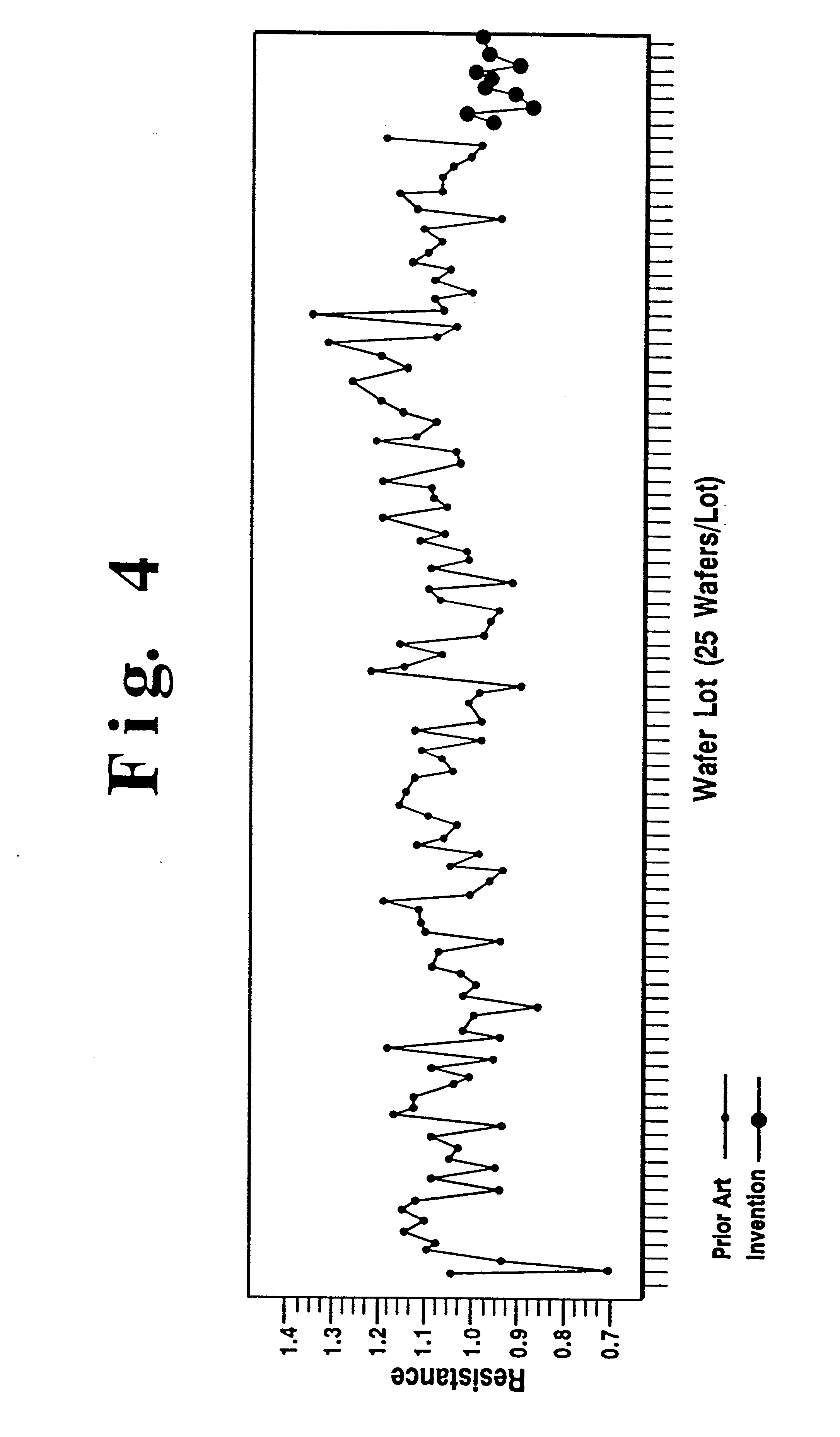
A CMP slurry for and method of polishing a semiconductor wafer during formation of metal interconnects are disclosed. The present invention utilizes a first slurry comprising a first oxidizer, preferably ferric nitrate, to remove the excess metal of the metal interconnect but which leaves the metal residues on the surface of the wafer. A second slurry comprising another oxidizer, preferably potassium iodate solution, having a greater affinity to both the metal residue and the liner material than the underlying dielectric is used to remove the metal residue and liner material with significantly reduced scratching of the underlying dielectric. The more robust metal interconnects formed utilizing the present invention is effective in lowering the overall resistance of a wafer, reducing the number of shorts, and provides greater protection of the underlying dielectric. Overpolishing of the wafer and its associated problems are avoided.

Description

1. Field of the InventionThis invention relates to chemical mechanical planarization of integrated circuit surfaces, and in particular, to a composition and method of removing metal layers when forming interconnect structures. The composition and method of the present invention provides enhanced removal of residual metal and liner material from the interconnect structure while reducing scratching of the underlying dielectric layers.2. Description of Related ArtIntegrated circuits are chemically and physically integrated into a semiconductor substrate by patterning layers on the substrate. These layers can be conductive, for conductor and resistor fabrication. A thousand or more devices can be formed simultaneously on the surface of a single wafer of semiconductor material. It is essential for high device yields to start with a flat semiconductor wafer. If the process steps of device fabrication are performed on a wafer surface that is not planar, various problems can occur which may...

Claims


Application Information

Patent Timeline
IPC IPC(8): B24B37/00B24B7/22B24B7/20C09K3/14H01L21/02H01L21/304H01L21/321
CPCH01L21/3212Y02P80/30
Inventor CRUZ, JOSE L.HUYNH, CUC K.KRYWANCZYK, TIMOTHY C.STURTEVANT, DOUGLAS K.
Owner IBM CORP
Learn More