
Apparatus and method of layout generation, and program thereof

a technology of layout and generating apparatus, applied in the direction of program control, computer aided design, instruments, etc., can solve the problems of inability to increase the operation speed, the size of the transistor increases infinitely, and the power consumption might increase by through curren

Inactive Publication Date: 2003-06-24
RENESAS ELECTRONICS CORP
View PDF11 Cites 13 Cited by
  • Summary
  • Abstract
  • Description
  • Claims
  • Application Information

AI Technical Summary

Benefits of technology

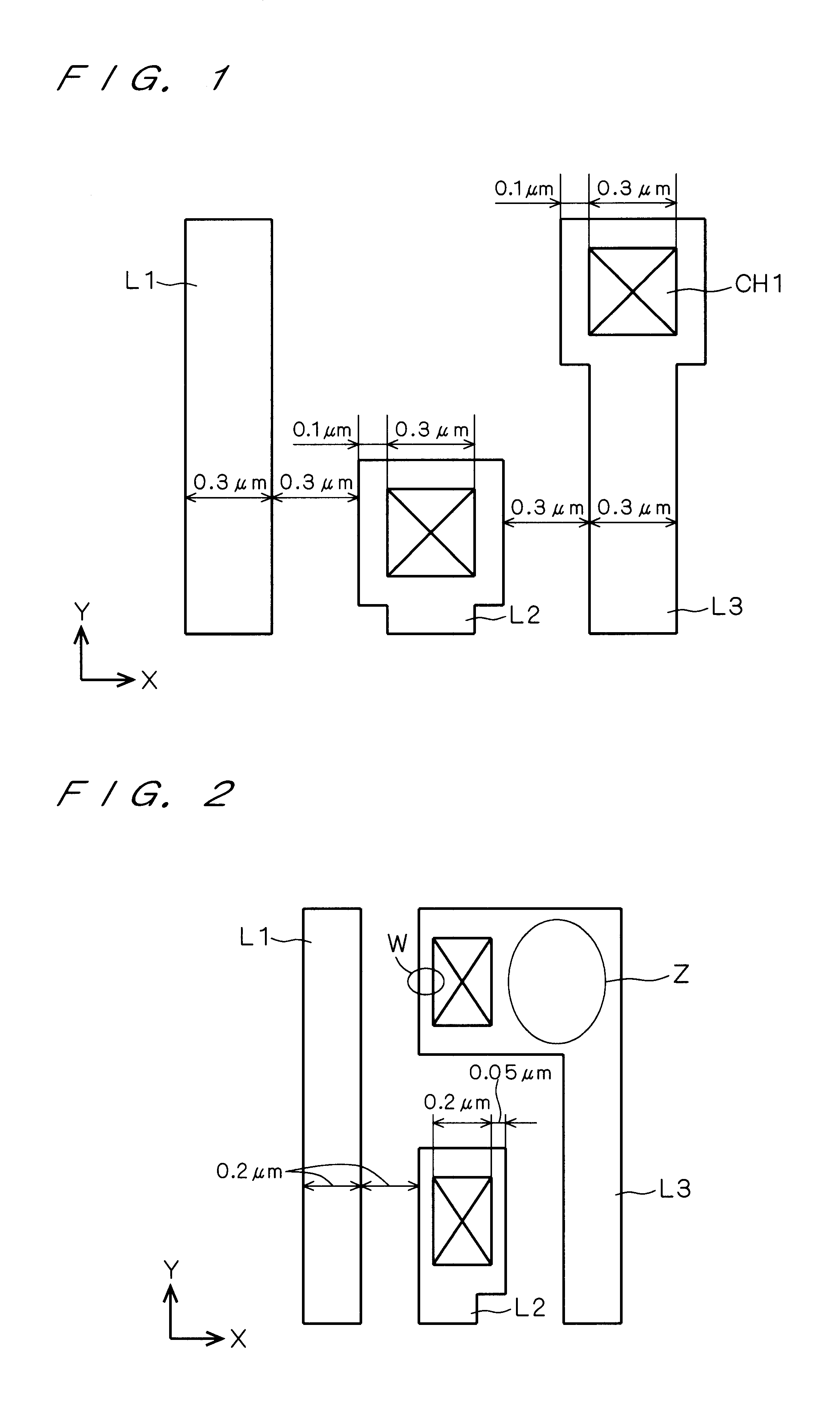
Problems in the layout of FIG. 2 are regions W and Z. That is, in the region W, the cover margin between the contact portion CH1 and the wiring L3 is the minimum value (0.05 .mu.m). In general, however, the cover margins of slightly larger than the minimum value can reduce contact resistance and improve yield.

Problems solved by technology

In terms of improvements in the degree of integration, a smaller transistor is preferred, however, its operation speed cannot be increased.
Also, power consumption might increase by through current due to blunting of waveform.
Unless the maximum value is set, by the presence of a transistor occupying a large ratio of the layout area and exerting influence on operation speed and power consumption, the size of this transistor increases infinitely, resulting in a large layout area.
Therefore, the conventional techniques cannot accurately provide the upper limit value of a channel width at the time of optimization.
On the contrary, setting the upper limit to a small value decreases the degree of freedom of optimization, which causes the degradation of optimization (i.e., a drop in operation speed and an increase in power consumption on circuit).
As a result, there is no possibility that an excessive reduction of channel width causes a decrease or an increase in layout area, thus failing to achieve the target layout area.
As a result, there is no possibility of failing to obtain a desired characteristic due to a channel-width optimization processing of low reliability.

Method used


Image

  • Apparatus and method of layout generation, and program thereof
  • Apparatus and method of layout generation, and program thereof
  • Apparatus and method of layout generation, and program thereof

Examples


Embodiment Construction

A-1. Configuration of Apparatus

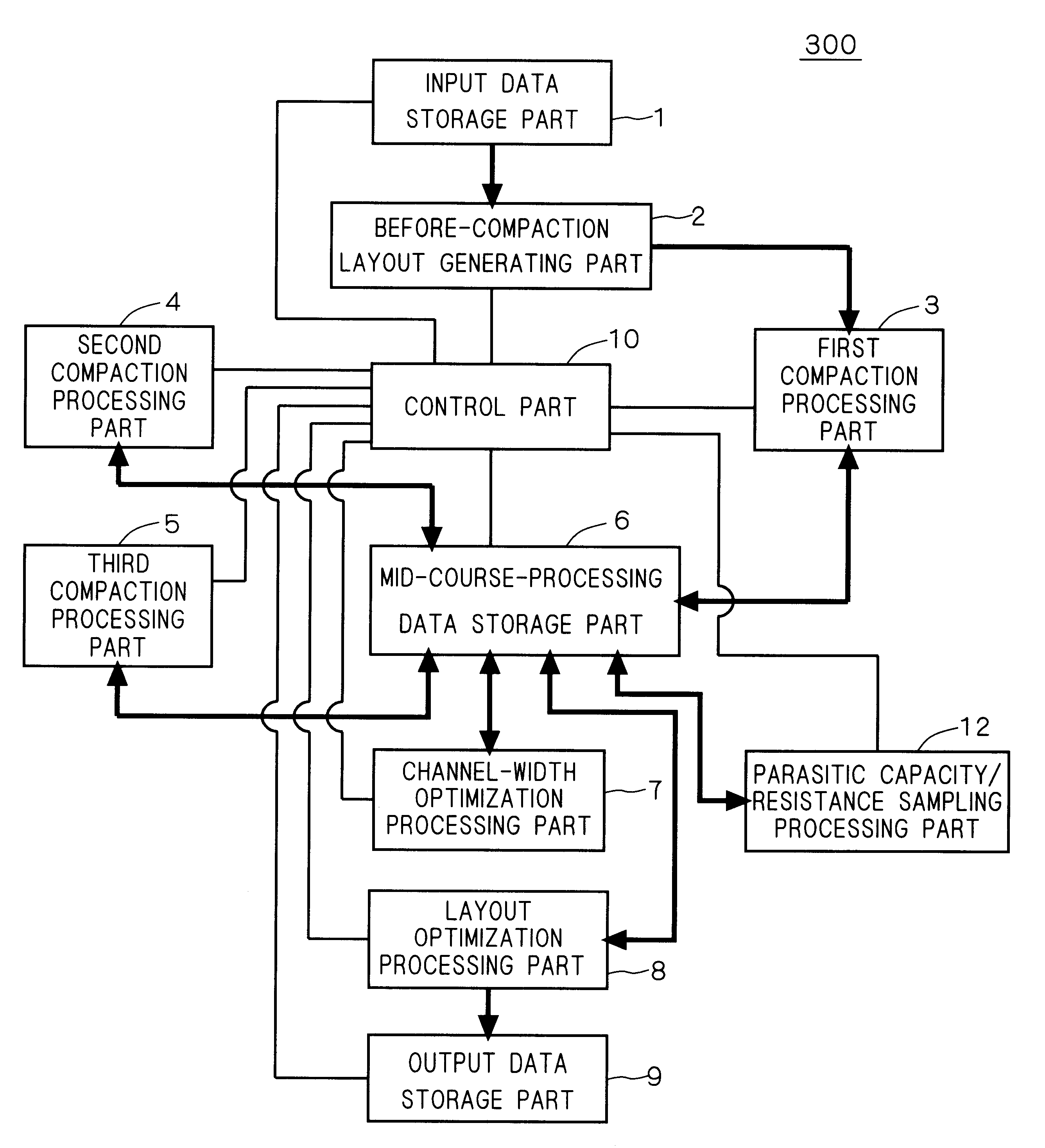
FIG. 4 shows the configuration of a layout generating apparatus 100, as a first preferred embodiment of the invention.

Referring to FIG. 4, the layout generating apparatus 100 comprises an input data storage part 1, before-compaction layout generating part 2, first compaction processing part 3, second compaction processing part 4, third compaction processing part 5, mid-course processing data storage part 6, channel-width optimization processing part 7, layout optimization processing part 8, output data storage part 9, and control part 10. The operations of these parts are controlled by the control part 10. In FIG. 4, bold arrows indicate the data flow among respective parts.

A-2. Operation of Apparatus

The procedure of layout generation is described with respect to FIG. 5 that is a flowchart of the operation of the layout generating apparatus 100, and the functions and operations of the respective parts are described by referring to FIG. 4.

In step S1 in ...


PUM


Abstract

A layout generating apparatus and a layout generating method to obtain high-quality optimization results (improvements in operation speed and the degree of integration and a reduction in power consumption). Specifically, there are disposed input data storage part (1), before-compaction layout generating part (2), first compaction processing part (3), second compaction processing part (4), third compaction processing part (5), mid-course-processing data storage part (6), channel-width optimization processing part (7), layout optimization processing part (8), output data storage part (9), and control part (10). The operations of all the mentioned parts are controlled by the control part (10).

Description

1. Field of the InventionThe present invention relates to a layout generating apparatus and a layout generating method of a semiconductor integrated circuit, as well as a program for directing a computer to execute the method.2. Description of the Background ArtIn designing semiconductor integrated circuits, there is increasing demand for improvements in the degree of integration, operation speed and power consumption of the circuits, whereas there is increasing demand for a reduction in design period. It is therefore required to improve the degree of integration, operation speed and power consumption in a short period of time.As technique of increasing the efficiency of and automatizing the layout designs of semiconductor integrated circuits, there are, for example, a method called "layout synthesis" to generate a layout based on a net list (i.e., a connected information of transistor level), and a method called "technology migration" to generate a layout of a desired design rule b...

Claims


Application Information

Patent Timeline
Patent Type & Authority Patents(United States)
IPC IPC(8): G06F17/50H01L21/82H01L21/822H01L27/04
CPCG06F17/5081G06F30/398
Inventor FUJII, TAKASHI
Owner RENESAS ELECTRONICS CORP
Learn More