D flip-flop structure with flush path for high-speed boundary scan applications
a flip-flop structure and boundary scan technology, applied in the field of integrated circuits, can solve the problems of circuit card testing expenses, circuit card testing fixtures are complex, and the expense of circuit card testing is larg
- Summary
- Abstract
- Description
- Claims
- Application Information
AI Technical Summary
Problems solved by technology
Method used
Image

Examples
Embodiment Construction
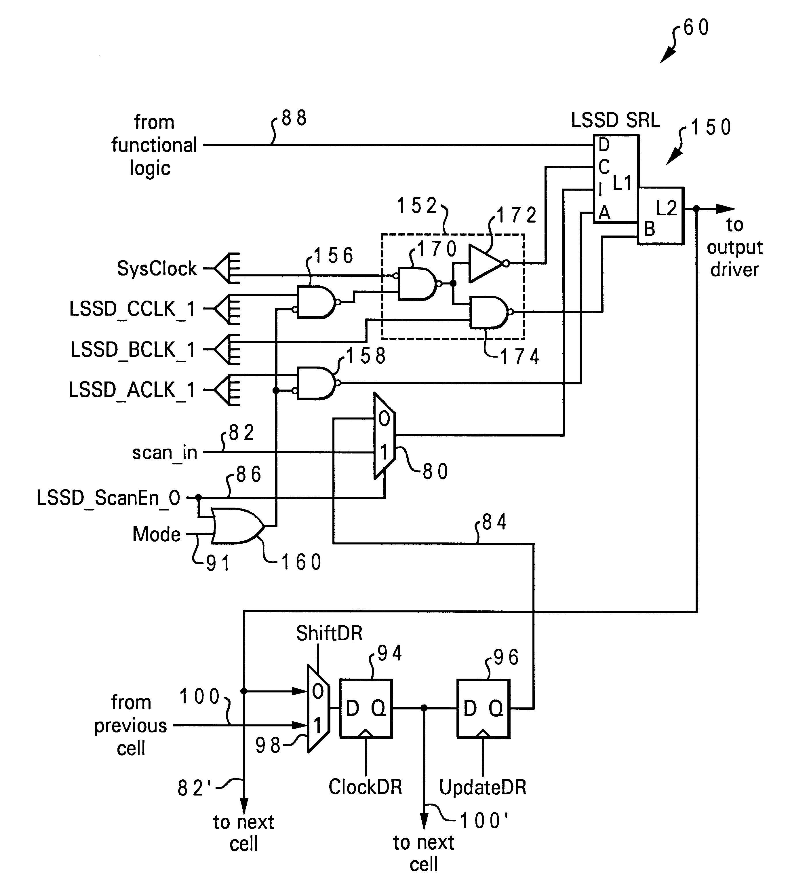
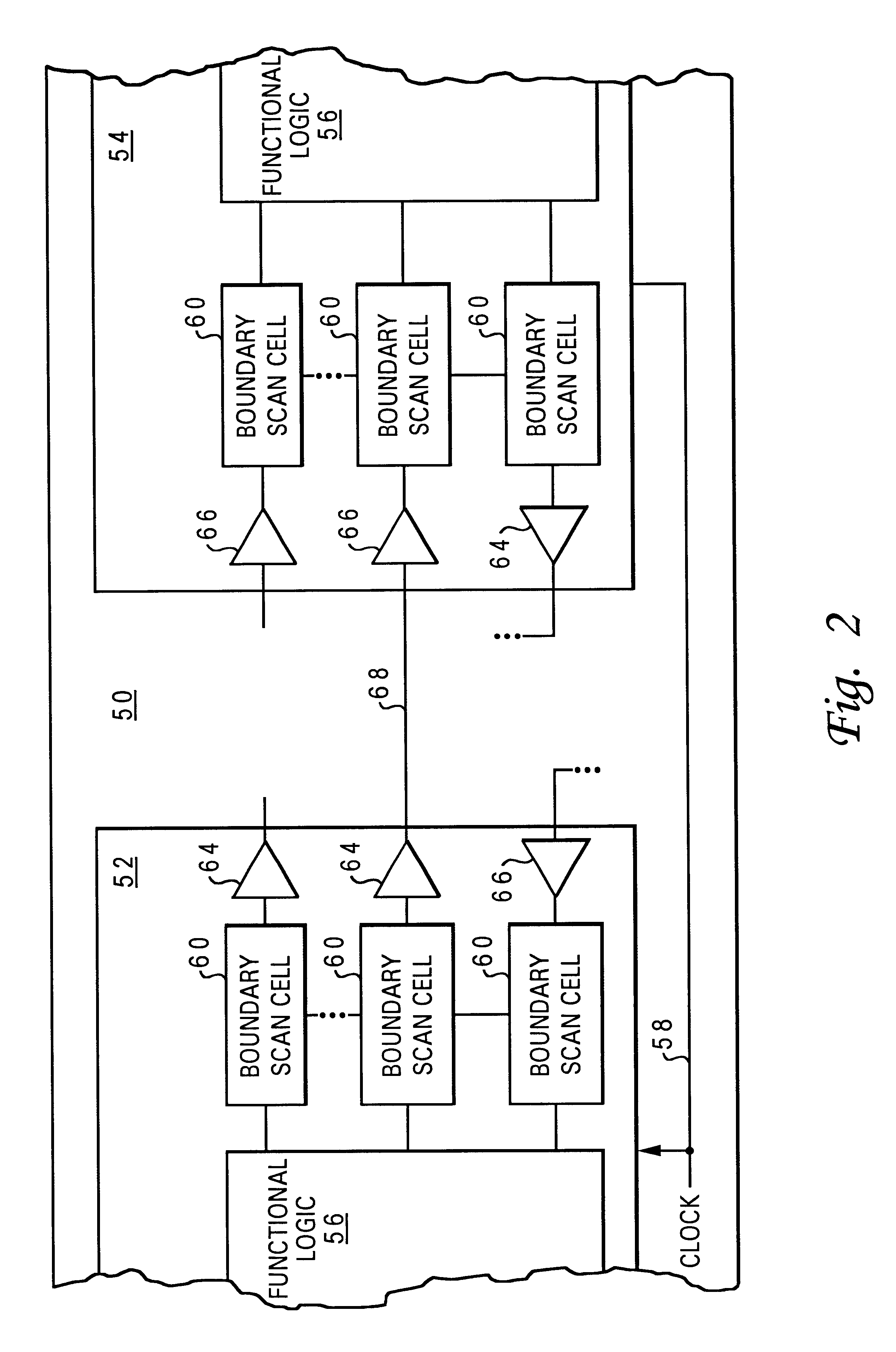
With reference again to the figures and in particular with reference to FIG. 2, there is depicted a high level block diagram of a circuit card 50 on which are mounted interconnected integrated circuit chips 52 and 54 in accordance with the present invention. The function of each of integrated circuit chips 52 and 54 is determined by its respective functional logic 56. For example, integrated circuit 52 may comprise a processor and integrated circuit chip 54 may comprise a cache memory, ASIC (Application Specific Integrated Circuit), or other support chip. In the illustrated embodiment, the operation of integrated circuit chips 52 and 54 is synchronized by clock signal 58.
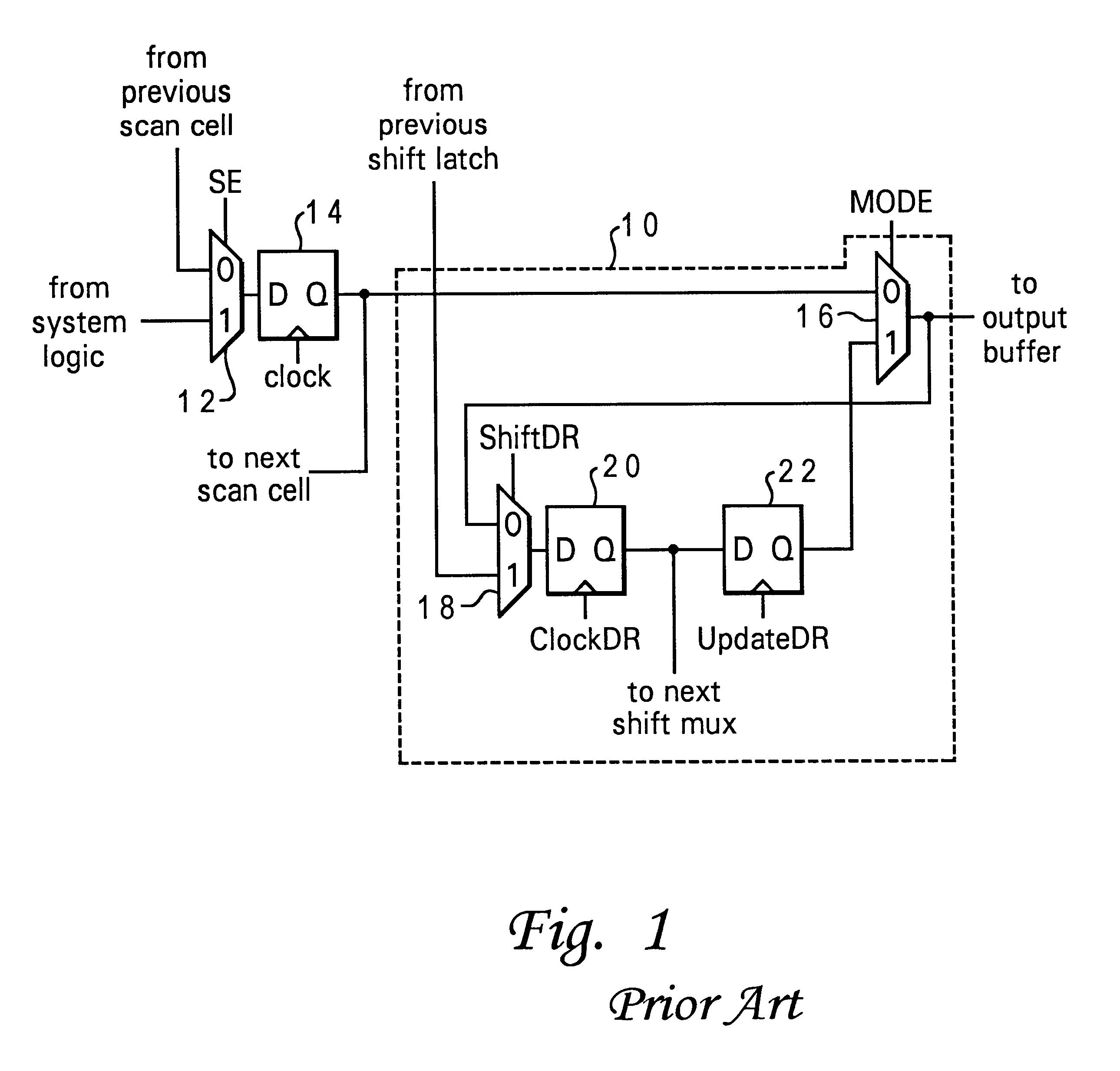
In accordance with the IEEE1149.1 standard, a respective IEEE1149.1-compliant boundary scan cell 60 is coupled, via a driver 64 or a receiver 66, between each of the input / output (I / O) pins of integrated circuit chips 52 and 54 and functional logic 56. Of course, for bi-directional I / O pins, the associated boundary ...
PUM
 Abstract
Description
Claims
Application Information
 - R&D
- Intellectual Property
- Life Sciences
- Materials
- Tech Scout
- Unparalleled Data Quality
- Higher Quality Content
- 60% Fewer Hallucinations
Browse by: Latest US Patents, China's latest patents, Technical Efficacy Thesaurus, Application Domain, Technology Topic, Popular Technical Reports.
© 2025 PatSnap. All rights reserved.Legal|Privacy policy|Modern Slavery Act Transparency Statement|Sitemap|About US| Contact US: help@patsnap.com