
Automatic defect source classification

a defect source and automatic technology, applied in the field of quality control, can solve problems such as the inability to determine the source of defects, the reduction of the sensitivity to defects caused by process variation inherent in semiconductor manufacturing, and the reduction of yield

Inactive Publication Date: 2003-01-14
GLOBALFOUNDRIES INC
View PDF10 Cites 45 Cited by
  • Summary
  • Abstract
  • Description
  • Claims
  • Application Information

AI Technical Summary

Benefits of technology

FIG. 6 shows a high-level logic flowchart of an example of the quantitativization process utilized b...

Problems solved by technology

One of the main causes of reduced yield is particle defects introduced during the manufacturing process.
The disadvantage is that they are expensive.
The disadvantage is reduced sensitivity to defects caused by process variation inherent in semiconductor manufacturing, and the inability to determine the source of the defects.
There are several problems associated with dispositioning, as dispositioning is performed in the art.
First, it takes roughly 6 months to 2 years to adequately train a human to do dispositioning.
Fourth, dispositioners, being human, are prone to human error, illness, lack of attention, etc.
Fifth, when a change is made in a production process, human dispositioners often have difficulty in responding to the change.

Method used


Image

  • Automatic defect source classification
  • Automatic defect source classification
  • Automatic defect source classification

Examples


Embodiment Construction

)

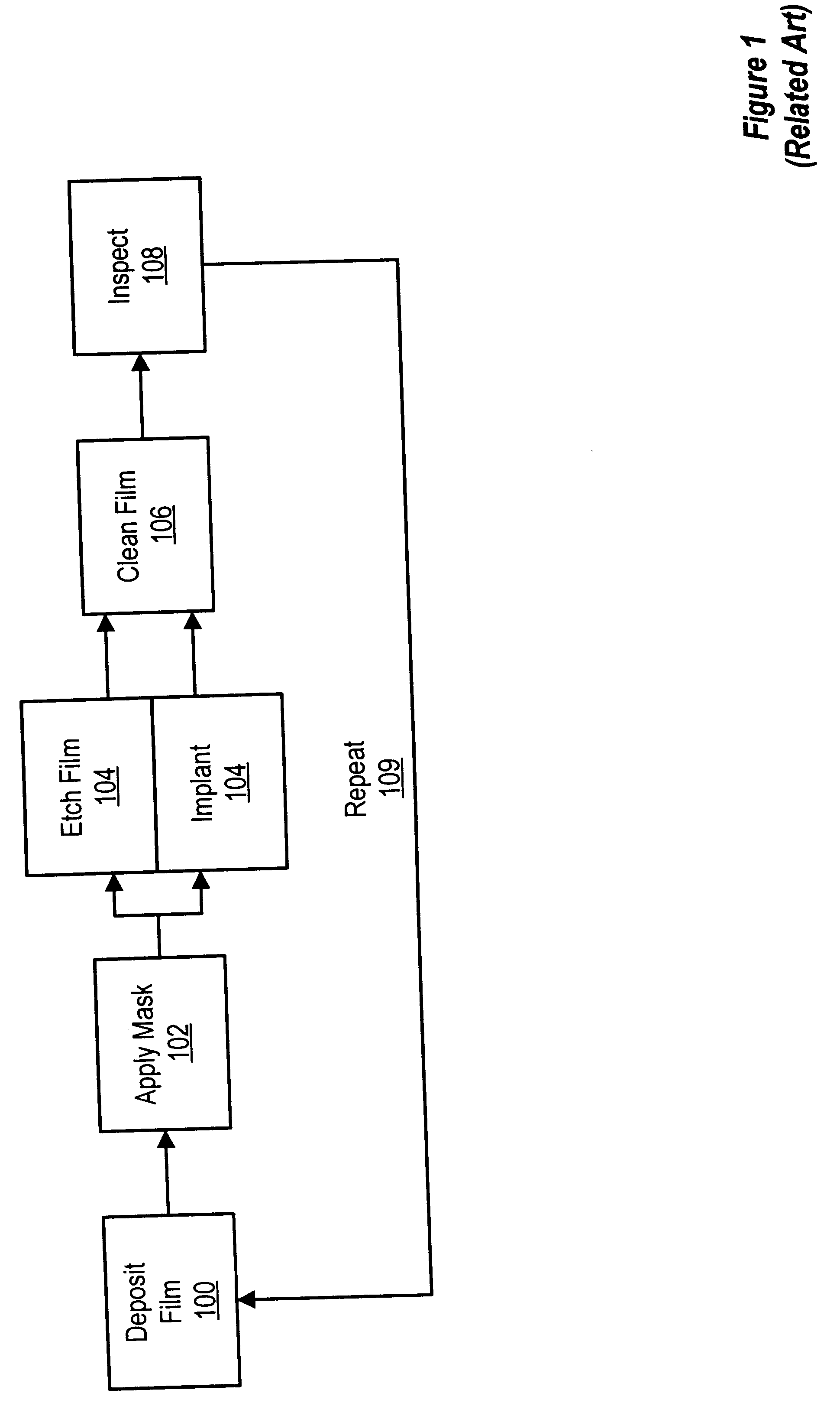
With reference to the figures, and in particular with reference now to FIG. 1, shown is a high-level flow diagram depicting a related-art process module by which integrated circuit wafers are manufactured. Depicted is that the first operation in production is for film to be deposited (or grown) 100 on a wafer. Thereafter, shown is that a mask is applied 102 to the wafer. Next, illustrated is that the wafer is etched to selectively remove material or implanted (with ions which will give the semiconductor wafer material the desired electrical characteristics) 104, at this point, the organic polymers of the photomask and / or polymer byproducts of the etch process must be removed from the wafer. Thereafter, remaining film is cleaned away 106. Finally, the wafer is inspected for defects 108. Thereafter, repetitive step 109 shows that the basic process module is repeated. Typically, many repetitions of the basic process module (or the basic process module with major or minor variations) a...


PUM


Abstract

A method and system for use in wafer fabrication quality control. The method and system make quantitative a qualitative integrated circuit wafer defect signature. In response to the quantitativize wafer fabrication defect signature, the method and system identify at least one cause of the defect signature.

Description

1. Field of the InventionThis invention relates to quality control in the field of integrated circuit wafer manufacturing and testing.2. Description of the Related ArtIntegrated circuit manufacturing and testing requires a high degree of quality control. An integrated circuit (IC) is a miniature electric circuit composed of hundreds to tens of millions of discrete electronic circuit elements (e.g., transistors, resistors, capacitors, or inductors). Multiple ICs are manufactured, or formed, on semiconductor wafers (also known as integrated circuit wafers), through a series of oxidations, implants, controlled deposition of materials, and selective removal of materials. Manufacturing integrated circuit wafers typically requires upwards of between two hundred and four hundred discrete manufacturing steps.Once the manufacturing process is complete, a wafer will be divided into individual die (or chips). Each functional die will be sold as an individual IC. The quality of the manufacturin...

Claims


Application Information

Patent Timeline
IPC IPC(8): H01L21/66
CPCH01L22/20
Inventor KIRSCH, TRAVIS D.HANCE, BRYON K.WEBB, CARROLL W.
Owner GLOBALFOUNDRIES INC
Learn More