
Dual-damascene interconnect structures and methods of fabricating same

a technology of interconnect structure and damascene, which is applied in the direction of basic electric elements, electrical equipment, semiconductor devices, etc., can solve the problems of copper migrating or diffused into silicon dioxide, and reducing the permeability of the bond

Inactive Publication Date: 2002-07-09
NEWPORT FAB
View PDF13 Cites 92 Cited by
  • Summary
  • Abstract
  • Description
  • Claims
  • Application Information

AI Technical Summary

Problems solved by technology

This localized pressure creates mechanical strain on the chemical bonds comprising the surface being polished, rendering the chemical bonds more susceptible to chemical attack by the slurry.
The use of Cu as interconnect metal in dual damascene IC devices gives rise to many difficulties and challenges.
For example, copper tends to migrate or diffuse into the silicon dioxide, where it acts to increase leakage currents or actually short-out adjacent conductors.
In addition, once Cu diffuses through the silicon dioxide and reaches the silicon devices, the device will generally malfunction in some manner.
TiN, which is popular as a barrier layer in Al / W interconnect structures, is generally unsatisfactory for use with advanced copper interconnect structures.
First, it has been found that TiN exhibits inferior resistance to copper migration.
Second, TiN is not compatible with current Cu plating techniques used in Cu deposition due to, among other things, problems with adhesion of the Cu to TiN.
Specifically, Cu is plated directly on TiN along the wafer edge with poor adhesion.
Unfortunately, however, CVD TaN / Ta suffers from low deposition rate and high deposition temperature (i.e., temperatures greater than 500.degree. C.).
These high temperatures and low deposition rates are incompatible with current interconnect processes as well as future processes incorporating low-k dielectrics.
Even in the case where an ionized PVD process is used, high aspect ratio interconnects are prone to poor step coverage of the barrier layer at the sidewall of the vias.
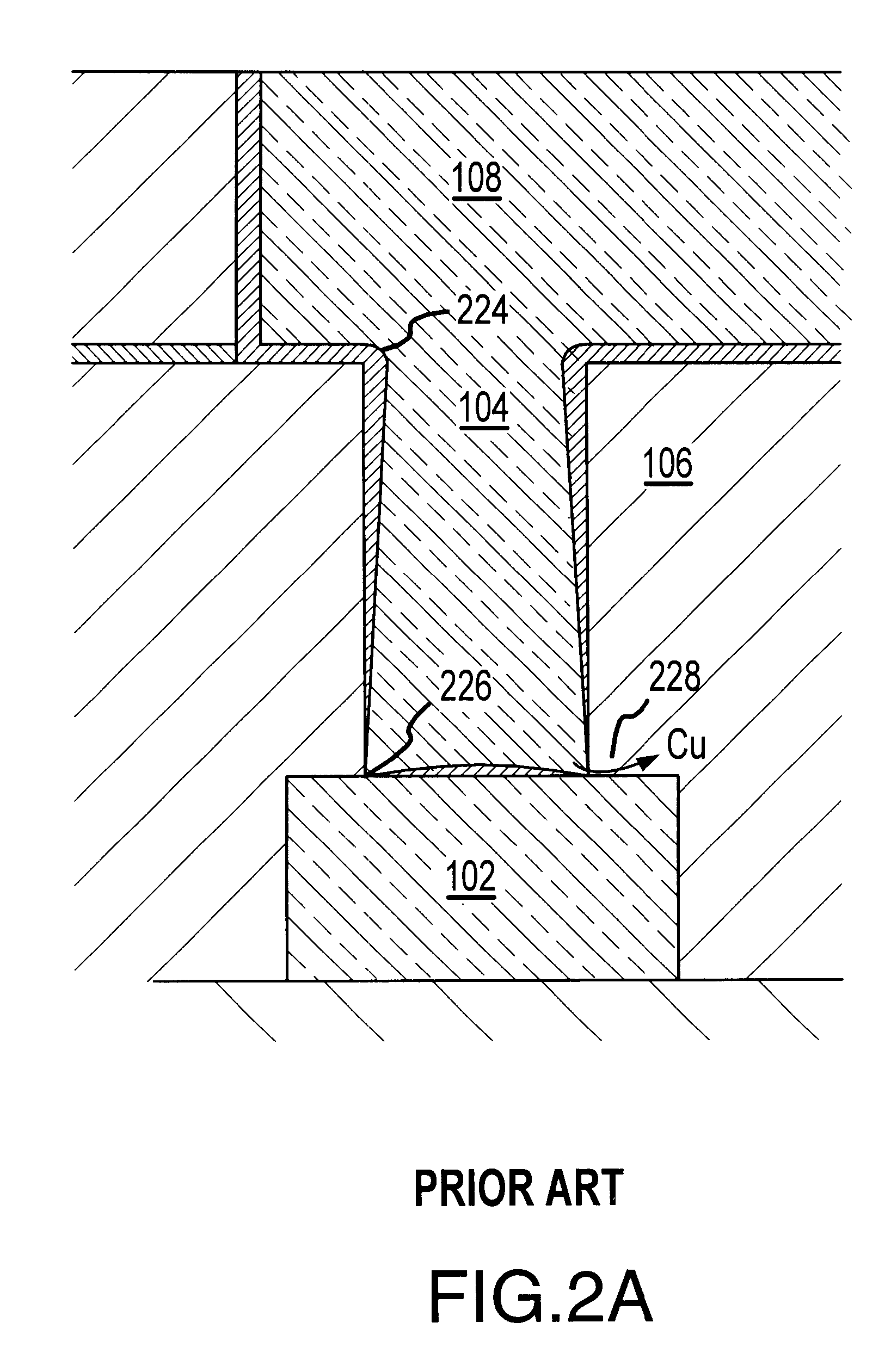
As mentioned above, this copper may then diffuse into surrounding structures, leading to significant reliability problems.
In addition, etching of high aspect ratio (AR) dual-damascene features is itself very challenging.
Although etching dielectrics is generally easier than etching metals (thus the desirability of damascene processes), as the lateral feature size of interconnects continue to shrink, etching the dual damascene structures of very high AR features leads to fabrication difficulties.
The absence of dielectric barrier along the interconnect trench sidewalls leads to low interconnect resistance and low interconnect capacitance.

Method used


Image

  • Dual-damascene interconnect structures and methods of fabricating same
  • Dual-damascene interconnect structures and methods of fabricating same
  • Dual-damascene interconnect structures and methods of fabricating same

Examples


Embodiment Construction

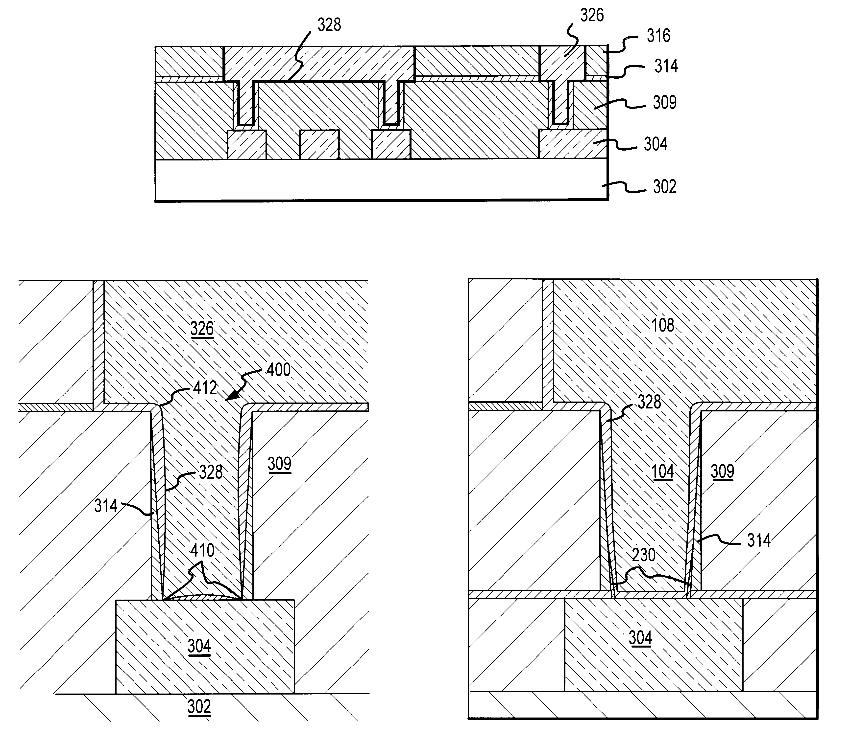
An interconnect fabrication process in accordance with various aspects of the present invention provides barrier enhancement at the via sidewall and improved capability to fabricate high aspect ratio dual damascene structures. While the manner in which the present invention addresses limitations of the prior art are discussed in detail below, in general, referring momentarily to FIG. 4, a via structure 400 formed within a dielectric 309 (linking metal pattern 326 and conductor 304), is lined with a barrier dielectric layer 314 (for example, silicon nitride) prior to deposition of metal barrier 328 onto the dual damascene structure. As a result, the effective barrier thickness along the bottom of the via (410) as well as the top of the via (412) is sufficient to eliminate the structure's susceptibility to Cu migration.

Referring now to the flowchart shown in FIG. 5, an exemplary method of practicing the present invention will now be described in conjunction with the cross-sectional di...


PUM

PropertyMeasurementUnit
feature sizesaaaaaaaaaa
dielectric constantaaaaaaaaaa
heightaaaaaaaaaa

Abstract

An interconnect fabrication process and structure provides barrier enhancement at the via sidewalls and improved capability to fabricate high aspect ratio dual damascene interconnects. A via structure is patterned into the via dielectric first, then a dielectric barrier (for example, anisotropically etched silicon nitride) is formed only along the via sidewalls in the dual damascene structure prior to deposition of a metal barrier (for example, Ta / TaN). In this way, the effective barrier thickness along the bottom of the via is increased, eliminating the structure's susceptibility to metal migration. The absence of dielectric barrier along the interconnect trench sidewalls leads to low interconnect resistance and low interconnect capacitance. The present invention also provides an improved fabrication method for obtaining high aspect ratio dual damascene interconnect structures.

Description

The present invention relates, generally, to methods and structures for improving the reliability and manufacturability of multilevel interconnects in integrated circuits and, more particularly, to a dual damascene process with barrier enhancement at the via sidewalls and improved capability for fabricating high aspect ratio interconnect structures.BACKGROUND ART AND TECHNICAL PROBLEMSThrough advanced semiconductor processing techniques, integrated circuit devices with sub-micron and sub-half-micron features sizes can now be manufactured. This trend toward deep submicron technology (i.e., involving feature sizes less than 0.35 microns) has, in turn, driven the need for multilayer interconnects. As a result, circuit performance in the deep submicron regime is increasingly a function of the delay time of electronic signals traveling between the millions of gates and transistors present on the typical integrated circuit chip. Parasitic capacitance and resistance effects resulting from ...

Claims


Application Information

Patent Timeline
Patent Type & Authority Patents(United States)
IPC IPC(8): H01L21/768H01L21/70
CPCH01L21/76808H01L21/76831H01L2221/1031
Inventor ZHAO, BINTSAU, LIMING
Owner NEWPORT FAB
Learn More