
Input/output methods for associative processor

a technology of associative processor and input/output method, which is applied in the direction of computing, instruments, and architectures with multiple processing units, can solve the problems of generating power consumption peak when used, inefficiency of prior art associative processors such as associative processor 10 and achieving speed enhancement

Inactive Publication Date: 2002-06-11
GSI TECH ISRAEL LTD
View PDF4 Cites 54 Cited by
  • Summary
  • Abstract
  • Description
  • Claims
  • Application Information

AI Technical Summary

Benefits of technology

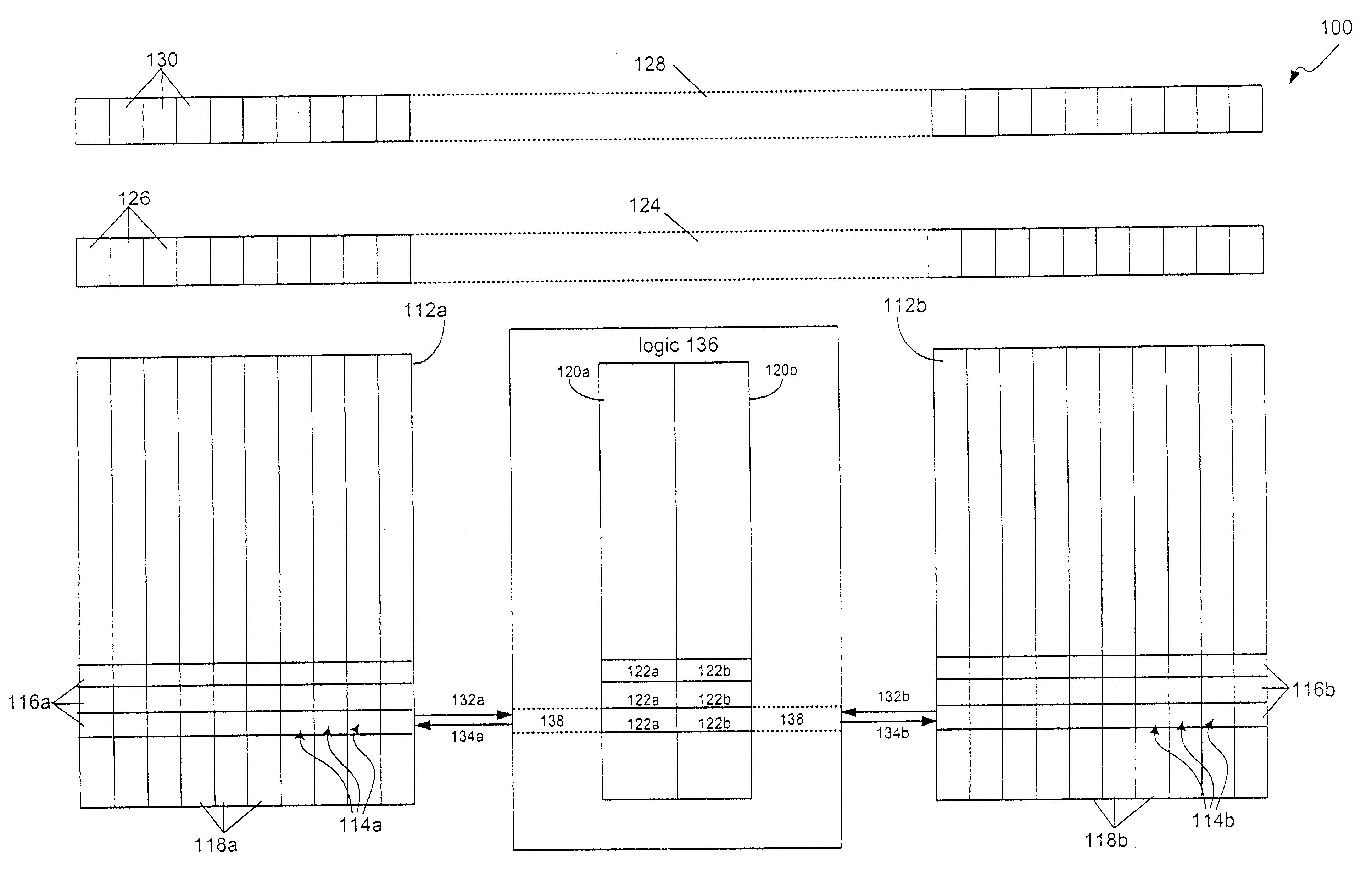
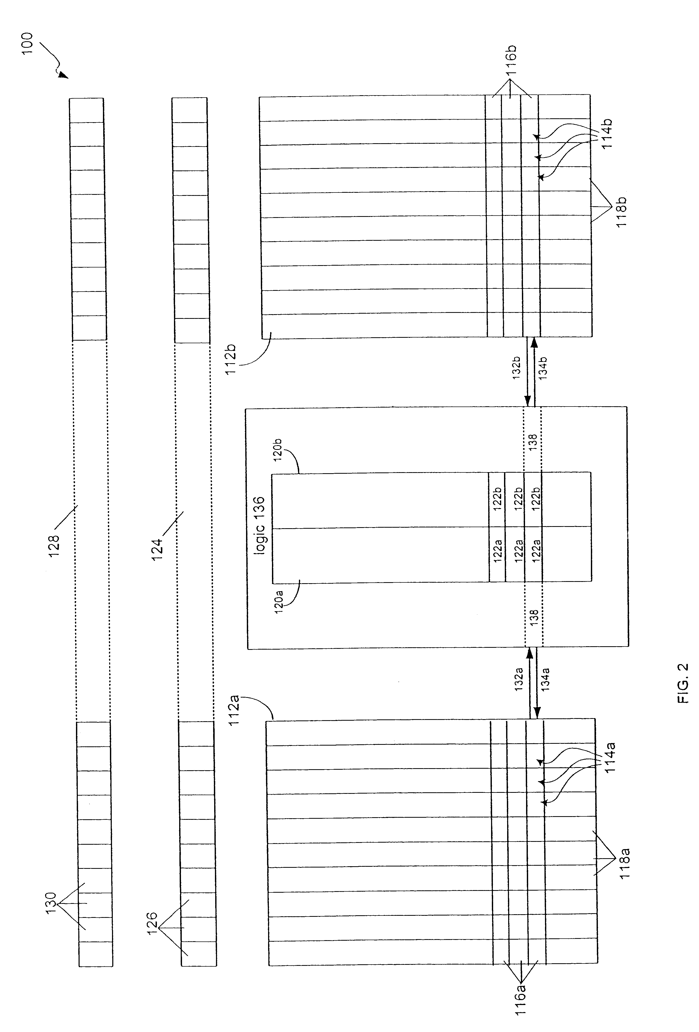
The ability to "mix and match" CAM cell arrays and tags registers enhances the efficiency with which the CAM cells of the present invention are used. To this end, the CAM cell arrays of the present invention typically have fewer columns than prior art CAM cell arrays. In fact, it is preferred that the sum of the number of columns of the CAM cell arrays of the present invention be equal to the number of columns needed by a prior art CAM cell array to perform all the contemplated arithmetical operations. For example, in an embodiment of the associative processor of the present invention that includes two CAM cell arrays, each with half as many columns as a prior art CAM cell array, two arithmetical operations that each require half the columns of the prior art CAM cell array are performed in parallel, with one of the arithmetical operations being performed with reference to one of the tags registers and another of the arithmetical operations being performed with reference to another of the tags registers. The two arithmetical operations may be either identical or different. To perform an arithmetical operation that requires the full width of a prior art CAM cell array, both CAM cell arrays of the present invention are associated with the same tags register, and the arithmetical operation is performed with reference to that tags register. Furthermore, arithmetical operations may be pipelined. To pipeline two sequential arithmetical operations, one CAM cell array is dedicated to the first operation and another CAM cell array is dedicated to the second operation. Compare operation cycles on the first CAM cell array are paired with write operation cycles on the second CAM cell array to transfer the output of the first operation from the first CAM cell array to the second CAM cell array for the second operation, with the same tags register being associated with the first CAM cell array for the compare operation cycles and with the second CAM cell array for the write operation cycles. In each elementary operation cycle pair, a column of the first CAM cell array, activated by appropriate bits in the corresponding mask and pattern registers, is copied to a column of the second CAM cell array, also activated by appropriate bits in the corresponding mask and pattern registers. Note that the mask and pattern registers are shared by all the CAM cell arrays.
The ability to "mix and match" CAM cell arrays and tags registers also facilitates another aspect of the present invention, the parallelization of input and output in a manner superior to that taught in U.S. patent application Ser. No. 09 / 140,411. For example, to process data stored in a memory simultaneously in two CAM cell arrays, as described above, one of the tags registers is designated as an input tags register. This input tags register is associated with one of the CAM cell arrays. Enough data bits to fill the input tags register are written from the memory to the input tags register, over the course of several machine cycles, using a bus with less bandwidth than is needed to fill the input tags register in one machine cycle. In each machine cycle, a control block selects the tag register cells of the input tags block that are to receive the data bits that are written from the memory to the input tags block during that machine cycle. After the tags register is filled, a write operation cycle is used to write these bits to a column of the target CAM cell array. This is repeated until as many columns of the CAM cell array as required have received the desired input. Then the input tags register is associated with a different CAM cell array. Another set of data bits is written from the memory to the input tags register, and a write operation cycle again is used to write these bits to a column of the second CAM cell array. This is repeated until as many columns of the second CAM cell array as required have received the desired input.
As many bits as there are rows of CAM cells in the associative processor are exchanged between the buffer and a target column of the associative processor in one elementary operation (compare or write) cycle. This is much faster than the one data element per elementary operation cycle of the prior art serial input / output method. This enhanced speed enables yet another aspect of the present invention. Because the rows of the CAM cell arrays of the present invention typically are shorter than the rows of prior art CAM cell arrays, an arithmetical operation executed on one of the CAM cell arrays may produce columns of intermediate results that leave insufficient room in the CAM cell array for the execution of subsequent arithmetical operations. These columns of intermediate results are written to the random access memory, via the input / output buffer, for temporary off-line storage, with one column of intermediate results being written in one machine cycle. As described above in the context of the parallelization of input and output, the number of machine cycles needed to transfer a column of intermediate results from the input / output buffer to the random access memory, or vice versa, depends on the bandwidth of the bus that connects the input / output buffer to the random access memory. When these columns of intermediate results are again needed, they are retrieved from the random access memory, also via the input / output buffer.

Problems solved by technology

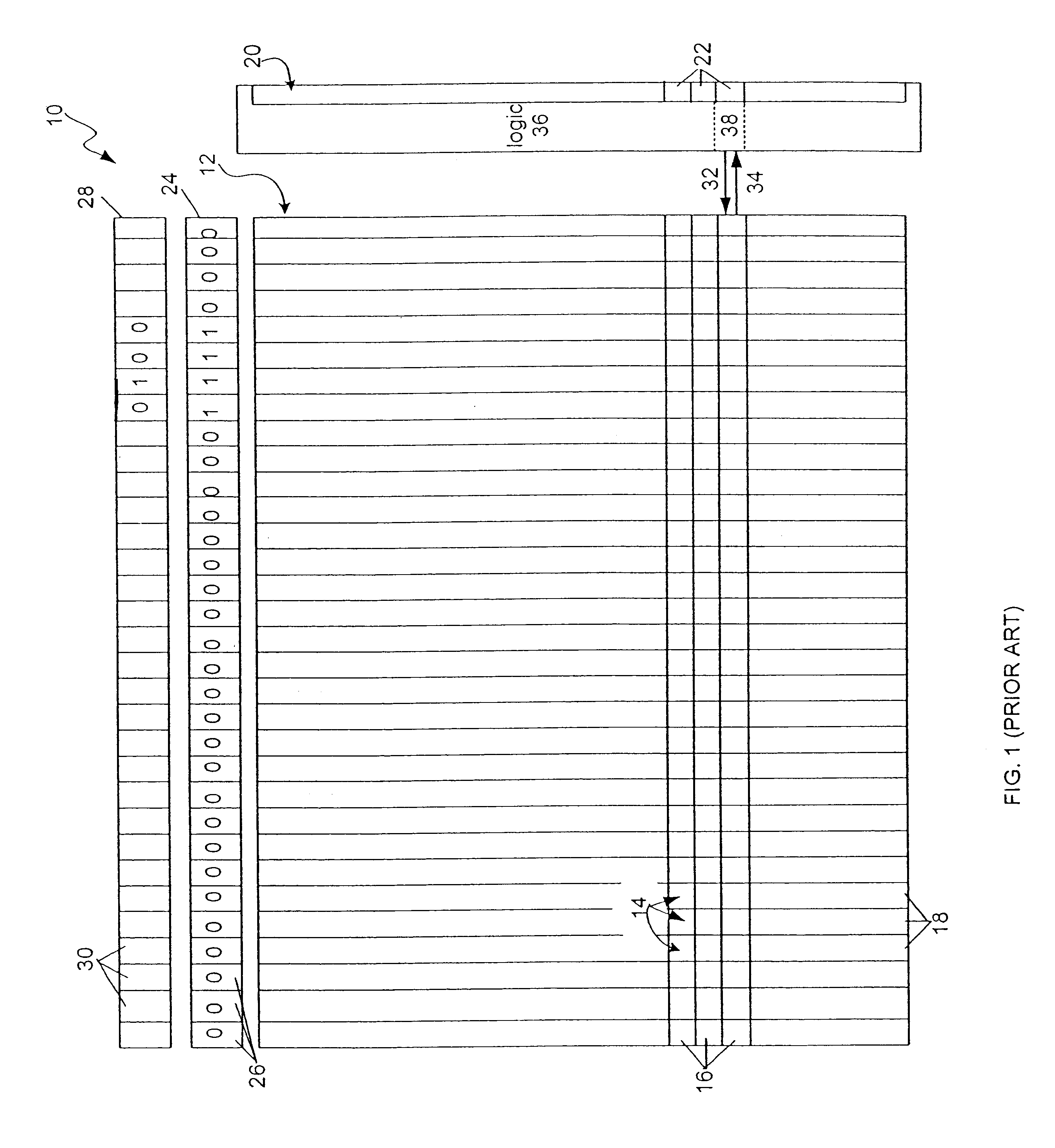
Nevertheless, prior art associative processors such as associative processor 10 suffer from certain inefficiencies.
In addition, although such a bus would be used for only a small fraction of the overall processing time, such a bus would generate power consumption peaks when used.

Method used


Image

  • Input/output methods for associative processor
  • Input/output methods for associative processor
  • Input/output methods for associative processor

Examples


Embodiment Construction

The present invention is of an associative processor that operates more efficiently than prior art associative processors, and of methods for its use. The present invention can be used for efficient processing of limited precision digital data such as eight-bit digital images.

The principles and operation of an associative processor according to the present invention may be better understood with reference to the drawings and the accompanying description.

Referring now to the drawings, FIG. 2 is a schematic illustration of an associative processor 100 of the present invention. Similar to prior art associative processor 10, the heart of associative processor 100 is two arrays 112a and 112b of CAM cells 114a and 114b. In array 112a, CAM cells 114a are arranged in rows 116a and columns 118a. In array 112b, CAM cells 114b are arranged in rows 116b and 118b. Associative processor 100 also includes four registers for controlling CAM cells 114a and 114b: two tags registers 120a and 120b that...


PUM


Abstract

A data processing device includes an associative processor that in turn includes one or more arrays of content addressable memory (CAM) cells and two or more tags registers. The device also includes a memory for storing the data and a bus for exchanging the data with the associative processor. During input and output operations, data are exchanged in parallel, via one of the tags registers. Another tags register is used to select rows of CAM cells for input or output. By appropriately shifting the bits in the buffer tags register between write or compare operation cycles, entire words are exchanged between the selected CAM cell rows and the buffer tags register. During arithmetical operations, in an embodiment with multiple CAM cell arrays, different tags registers are associated with different CAM cell arrays at will. If, in the course of performing arithmetical operations using one of the CAM cell arrays, so many columns of intermediate data are produced that insufficient columns remain for subsequent arithmetical operations, the columns of intermediate data are written to the memory, via the buffer tags registers. These columns of intermediate data are retrieved subsequently from the memory as needed, also via the buffer tags register.

Description

FIELD AND BACKGROUND OF THE INVENTIONThe present invention relates to associative processors and, more particularly, to an associative processor configured to perform two or more different arithmetical operations simultaneously and methods for loading the associative processor with data to be processed and for downloading the data after processing.An associative processor is a device for parallel processing of a large volume of data. FIG. 1 is a schematic illustration of a prior art associative processor 10. The heart of associative processor 10 is an array 12 of content addressable memory (CAM) cells 14 arranged in rows 16 and columns 18. Associative processor 10 also includes three registers for controlling CAM cells 14: a tags register 20 that includes many tag register cells 22, a mask register 24 that includes many mask register cells 26, and a pattern register 28 that includes many pattern register cells 30. Each cell 14, 22, 26 or 30 is capable of storing one bit (0 or 1). Ta...

Claims


Application Information

Patent Timeline
Patent Type & Authority Patents(United States)
IPC IPC(8): G06F12/00
CPCG06F15/8038
Inventor AKERIB, AVIDAN
Owner GSI TECH ISRAEL LTD
Learn More