


Quick Research
Generate reliable direction feasibility study reports for your R&D in just a few steps.

Technical Q&A
Discover and master advanced knowledge NOW. Basics, ideas, possibilities, all at once.

Find Solutions
As an expert in R&D theories, this can generate solutions to your technical problems instantly.

Evaluate Feasibility
Analyze your overall solution with one click, know your potential R&D risks in advance.

Monitor Landscape
Get weekly tech updates, stay abreast of the latest tech innovations and key insights.
Electronic device
- Summary
- Abstract
- Description
- Claims
- Application Information
AI Technical Summary
Problems solved by technology
Method used
Image

Examples
embodiment 1
[Embodiment 1 ]
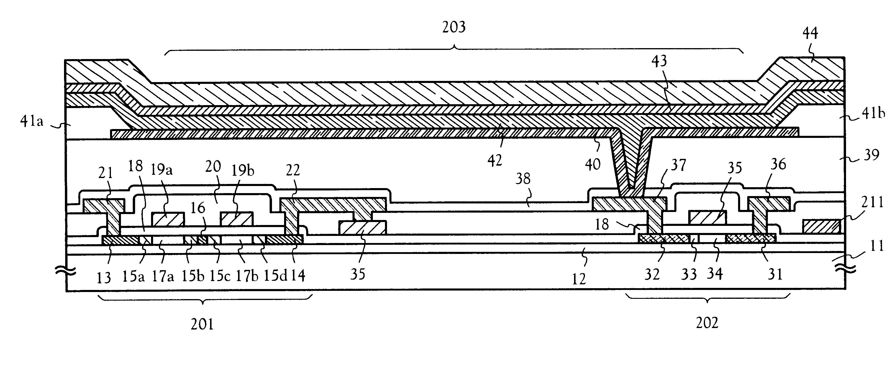
The embodiments of the present invention are explained using FIGS. 3A to 5C. A method of simultaneous manufacture of a pixel portion, and TFTs of a driver circuit portion formed in the periphery of the pixel portion, is explained here. Note that in order to simplify the explanation, a CMOS circuit is shown as a basic circuit for the driver circuits.
First, as shown in FIG. 3A, a base film 301 is formed with a 300 nm thickness on a glass substrate 300. Silicon nitride oxide films are laminated as the base film 302 in this embodiment. It is good to set the nitrogen concentration at between 10 and 25 wt % in the film contacting the glass substrate 300. Further, it is advantageous to provide the base film with a heat radiation function, a DLC (diamond like carbon) film can also be provided.
Next, an amorphous silicon film (not shown in the figures) is formed with a thickness of 50 nm on the base film 301 by a known deposition method. Note that it is not necessary to limit t...
embodiment 2
[Embodiment 2]
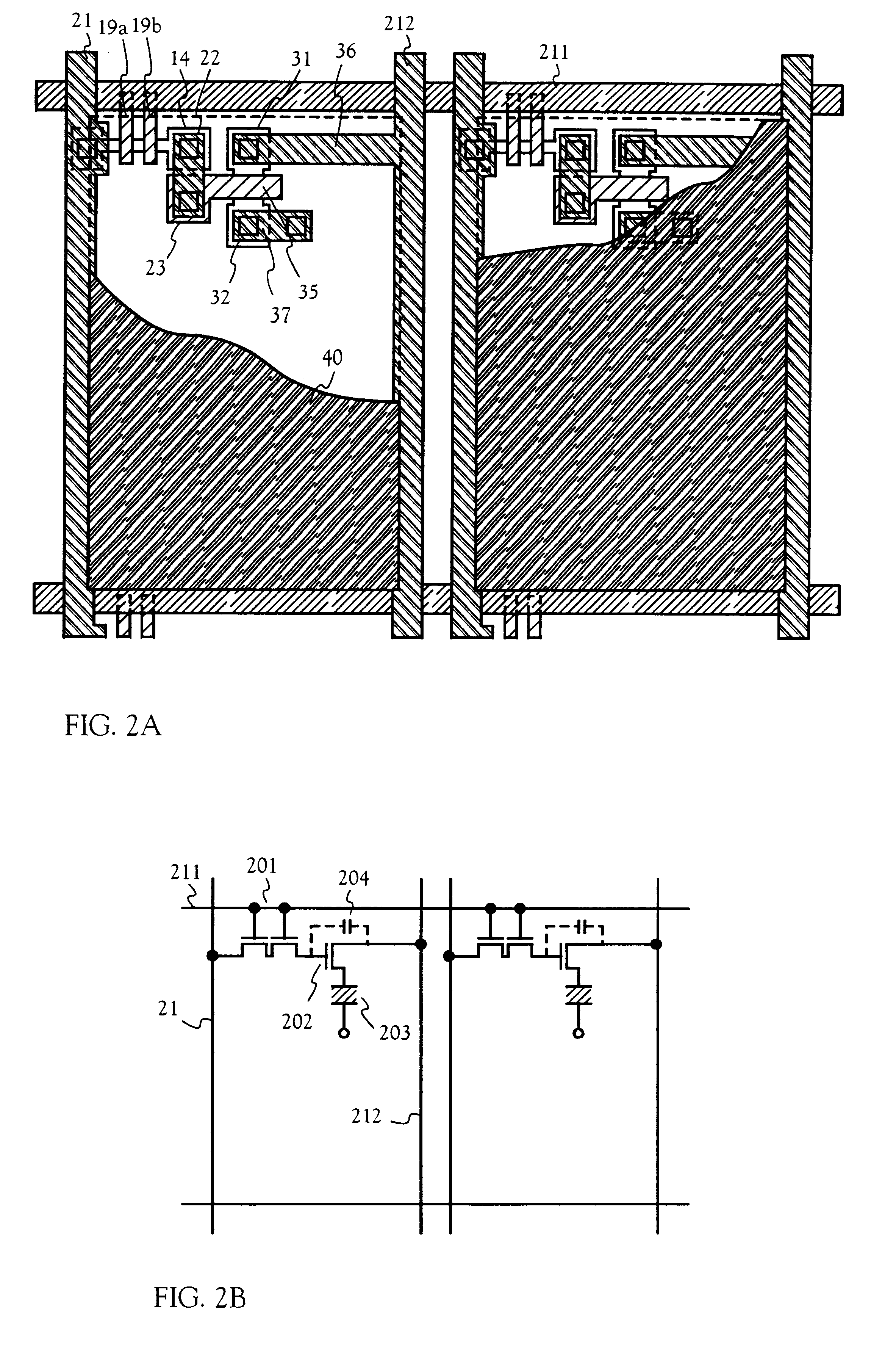
In this embodiment, an example of a case in which a pixel constitution shown in FIG. 9 differs from that of the circuit diagram (constitution) shown in FIG. 2B. Note that in this embodiment, reference numeral 901 denotes source wiring of a switching TFT 902, 903 denotes a gate wiring of a switching TFT 902, 904 denotes a current control TFT, 905 denotes a capacitor, 906 and 908 denote electric current supply lines, and 907 denotes an EL element.
It is to be noted that the capacitor 905 employs a gate capacitance of the current control TFT 904. Substantially, the capacitor 905 is not provided, and therefore it is indicated by a dotted line.
FIG. 9A is an example of a case in which the electric current supply line 906 is common between two pixels. Namely, this is characterized in that the two pixels are formed having linear symmetry around the electric current supply line 906. In this case, the number of the electric current supply line can be reduced, and therefore the pi...
embodiment 3
[Embodiment 3]
In this embodiment, examples in which the element structure of the electric current controlling TFT 202 shown in FIG. 1 is made a different one, will be described with reference to FIGS. 10A to 10D. Specifically, examples in which the arrangement of the LDD region is made a different one, will be described. Incidentally, the same portions as those of the electric current controlling TFT 202 shown in FIG. 1 are designated by the same symbols.
An electric current controlling TFT 202A shown in FIG. 10A is an example in which the LDD region 33 is omitted from the electric current controlling TFT 202 shown in FIG. 1. In the case shown in FIG. 1, since the switching TFT 201 has a triple-gate structure, an off current value is very small, and if a digital driving system is used, the capacitance of a capacitor for holding the electric potential of the gate of the electric current controlling TFT 202A may be very small.
Thus, as shown in FIG. 10A of this embodiment, it is possibl...
PUM
 Abstract
Description
Claims
Application Information
 - R&D Engineer
- R&D Manager
- IP Professional
- Industry Leading Data Capabilities
- Powerful AI technology
- Patent DNA Extraction
Browse by: Latest US Patents, China's latest patents, Technical Efficacy Thesaurus, Application Domain, Technology Topic, Popular Technical Reports.
© 2024 PatSnap. All rights reserved.Legal|Privacy policy|Modern Slavery Act Transparency Statement|Sitemap|About US| Contact US: help@patsnap.com