Method of manufacturing a metal wiring in a semiconductor device

a manufacturing method and technology for semiconductor devices, applied in semiconductor devices, semiconductor/solid-state device details, electrical apparatus, etc., can solve the problems of underlying wiring alignment problem and the inevitable generation of upper wiring, and the above process still has severe problems

Inactive Publication Date: 2002-04-23
HYUNDAI ELECTRONICS IND CO LTD
View PDF2 Cites 0 Cited by
  • Summary
  • Abstract
  • Description
  • Claims
  • Application Information

AI Technical Summary

Problems solved by technology

At this time, as the semiconductor device is higher integrated, an alignment problem of the underlying wiring and the upper wiring is inevitably generated during the lithography process of forming a via hole.
The upper wiring is disconnected from the underlying wiring by the void B due to poor burial into the via hole having a large step coverage.
The problem in the above process is still severe in case of damascene process used to form a copper wiring.

Method used


Image

  • Method of manufacturing a metal wiring in a semiconductor device
  • Method of manufacturing a metal wiring in a semiconductor device
  • Method of manufacturing a metal wiring in a semiconductor device

Examples


Embodiment Construction

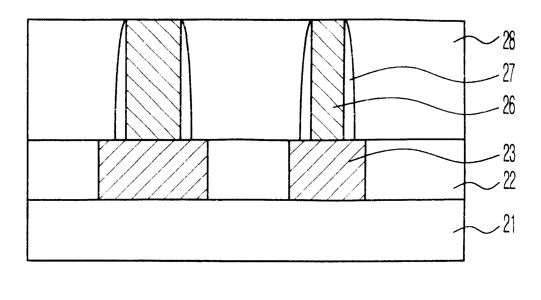
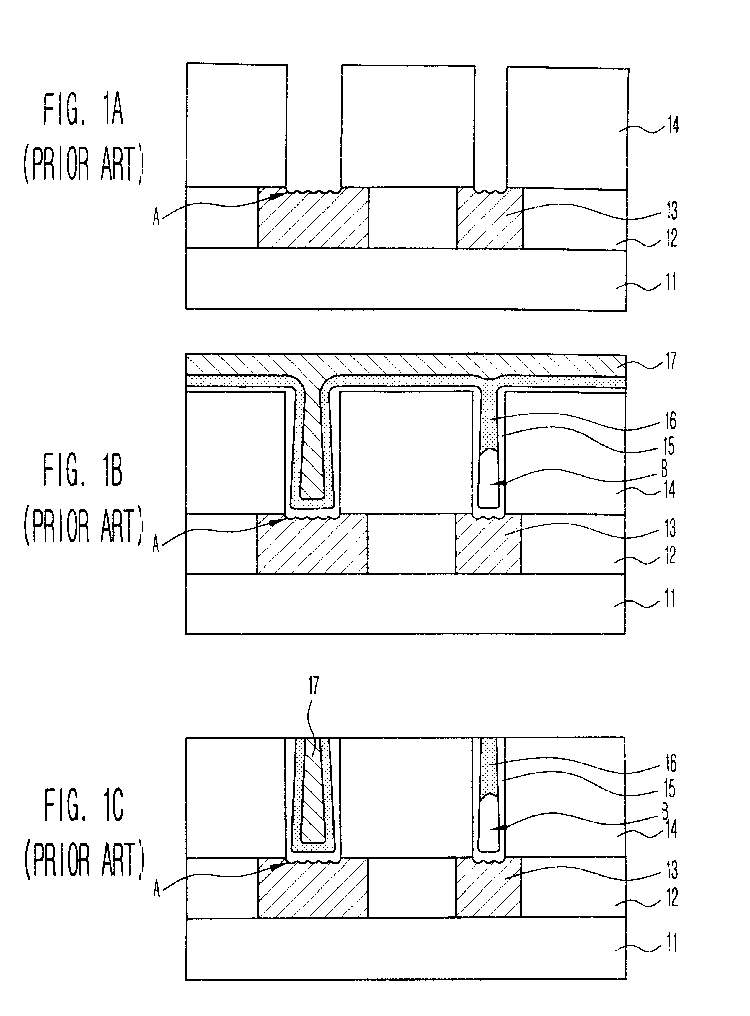
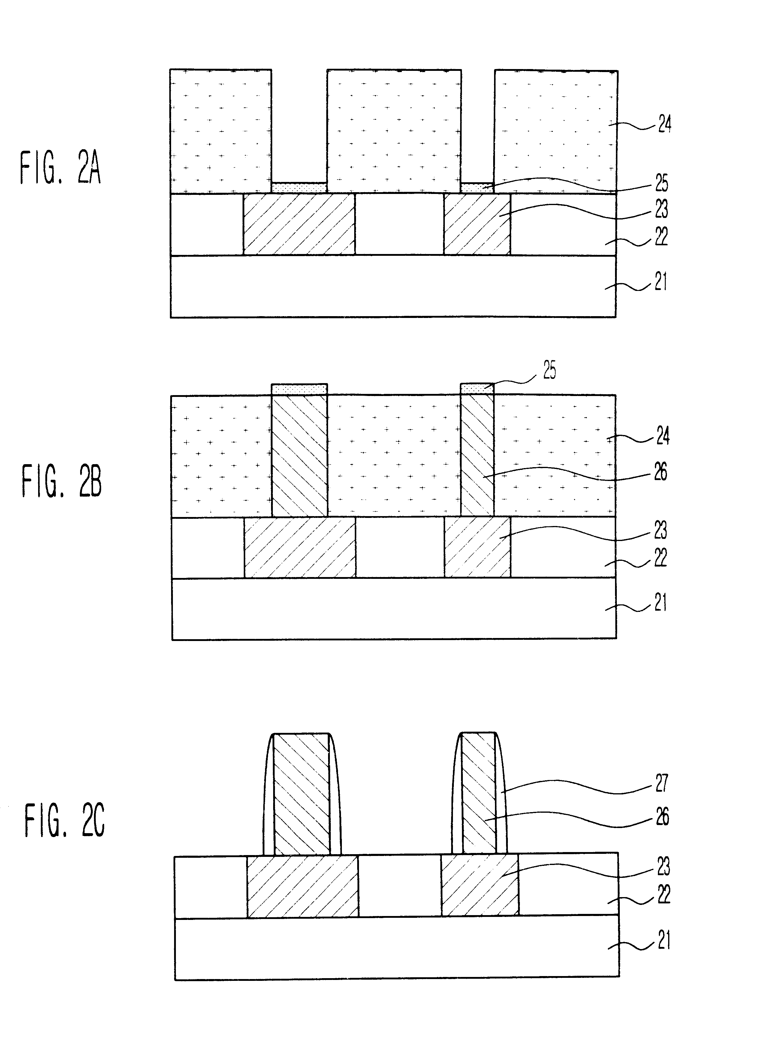
The disclosed methods will be described in detail by way of a preferred embodiment with reference to accompanying drawings. FIGS. 2A to 2D are cross-sectional views for explaining a method of manufacturing a metal wiring in a semiconductor device.

Referring now to FIG. 2A, a first insulating film 22 is formed on a semiconductor substrate 21 in which a given structure is formed. Then, after a given region of the first insulating film 22 is etched, a metal layer is formed on the etched region of the first insulating film 22 and is then patterned, thus forming an underlying metal wiring 23. After a photosensitive film 24 is formed with the same thickness to a desired height of the wiring, a portion in which an upper wiring will be formed is patterned to expose a portion of the underlying wiring 23. Then, a chemical enhancer 25, which is selectively adhered only to the exposed portion of the underlying metal wiring 23 without adhering to the photosensitive film 24, is deposited. The chem...


PUM

PropertyMeasurementUnit
temperatureaaaaaaaaaa
pressureaaaaaaaaaa
temperatureaaaaaaaaaa

Abstract

A method of manufacturing a metal wiring in a semiconductor device is disclosed. The method comprises forming a photosensitive film so that an underlying metal wiring can be exposed, adhering an chemical enhancer only to the underlying metal wiring, depositing a metal layer by CECVD method so that the metal layer is selectively deposited at the portion in which the chemical enhancer is formed, removing the photosensitive film and chemical enhancer, and forming a diffusion barrier layer spacer at the sidewall of the metal layer to form an upper metal wiring. Therefore, the disclosed method can solve poor contact with an underlying metal wiring due to shortage of processional margin in the process of forming an upper metal wiring in a high integration semiconductor device.

Description

1. Field of the Invention:The invention relates generally to a method of manufacturing a metal wiring in a semiconductor device. More particularly, the present invention relates to a method of manufacturing a metal wiring in a semiconductor device capable of solving the problem of poor contact with an underlying metal wiring due to shortage of processional margin in the process of forming an upper metal wiring in a semiconductor device.2. Description of the Prior Art:A method of manufacturing a conventional metal wiring in a semiconductor device will be explained below by reference to FIGS. 1A to 1C.Referring now to FIG. 1A, a first insulating film 12 is formed on a semiconductor substrate 11 in which a given structure is formed. Then, after a given region of the first insulating film 12 is etched, a metal layer is formed on the etched region of the first insulating film 12 and is then patterned, thus forming an underlying metal wiring 13. After a second insulating film 14 is formed...

Claims


Application Information

Patent Timeline
Patent Type & Authority Patents(United States)
IPC IPC(8): H01L21/4763H01L21/70H01L21/28H01L21/768H01L21/02H01L21/285
CPCH01L21/28562H01L21/76843H01L21/76885H01L21/76876H01L21/76852H01L21/28
Inventor PYO, SUNG GYU
Owner HYUNDAI ELECTRONICS IND CO LTD
Why Eureka
Try Eureka