Optical writing device

a writing device and optical writing technology, applied in the direction of printing, instruments, printing, etc., can solve the problem of the degree of precision with which the light from said mutually independent light signal emitting elements irradiates the surface of the image carrying member

Inactive Publication Date: 2001-08-21
MINOLTA CO LTD
View PDF13 Cites 0 Cited by
  • Summary
  • Abstract
  • Description
  • Claims
  • Application Information

AI Technical Summary

Problems solved by technology

A disadvantage arises, however, as to the degree of precision with which light from said mutu...

Method used


Image

  • Optical writing device
  • Optical writing device
  • Optical writing device

Examples


Embodiment Construction

The optical writing device of the present invention is not limited to the aforesaid embodiments and may be variously modified insofar as such modifications do not depart from the scope of the invention.

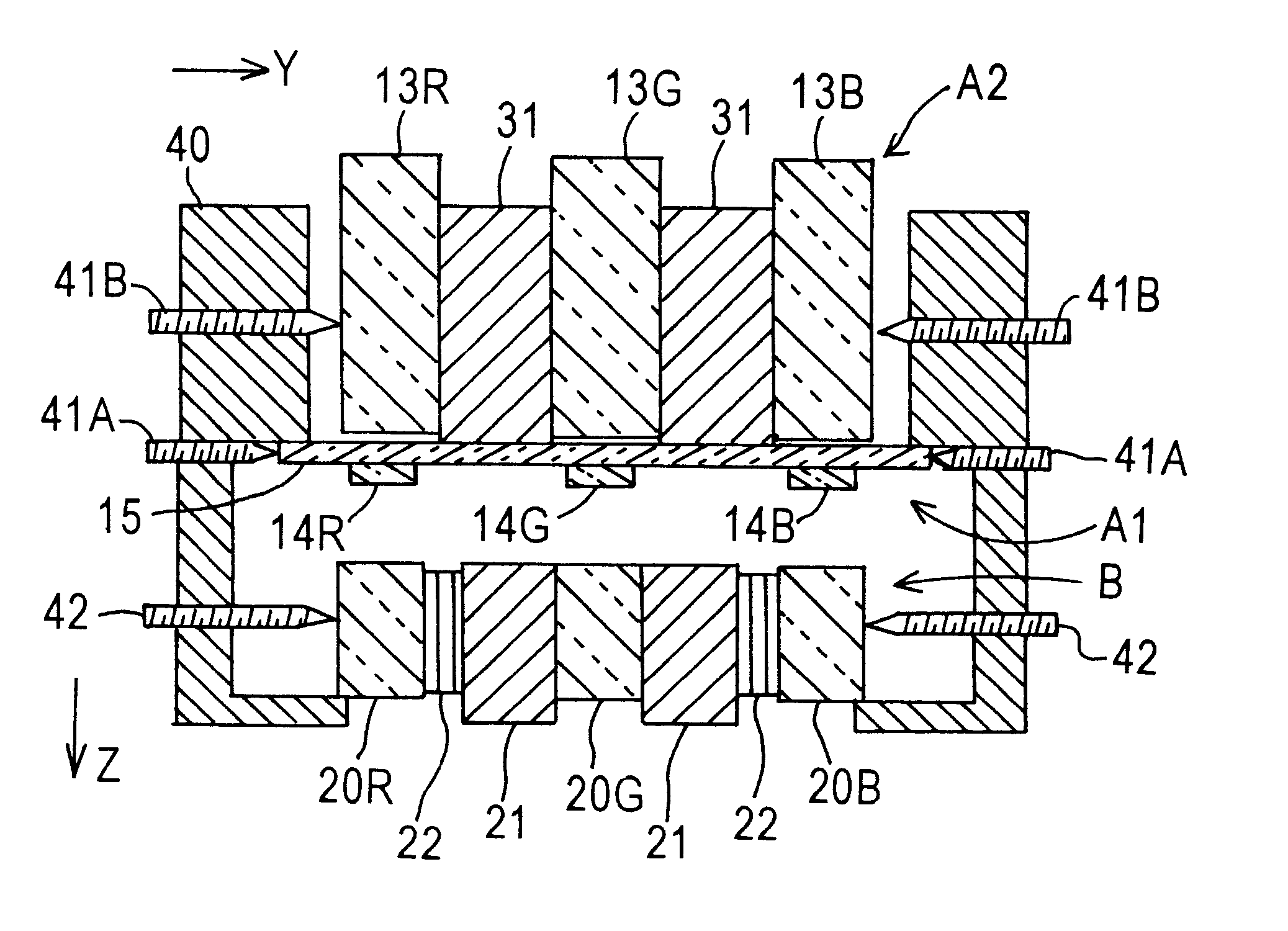
Specifically, light-emitting diode (LED), liquid crystal shutter (LCS), deformable mirror device (DMD), fluorescent device (FLD) and the like may be substituted for the PLZT solid-state scanning-type element. The present invention is not only applicable to image writing devices that write on paper using silver salt material, but may also be applied to image writing devices that write on silver salt film, and electrophotographic photosensitive members.

Although the present invention has been fully described by way of examples with reference to the accompanying drawings, it is to be noted that various changes and modification will be apparent to those skilled in the art. Therefore, unless otherwise such changes and modifications depart from the scope of the present invention, they should...


PUM


Abstract

Disclosed are optical writing devices each of which has three arrays of light shutter elements for emitting light signals of red, green and blue, respectively. The arrays of light shutter elements of each optical writing device are adjustably provided in an image forming apparatus with respect to sub-scan direction.

Description

1. Field of the InventionThe present invention relates to a solid-state scanning-type optical writing device for writing an image (latent image) on the surface of an image carrying member such as a photosensitive member, photosensitive paper or the like using a plumbus lanthanum zirconate titanate (PLZT) light shutter array, light-emitting diode (LED) array or the like.2. Description of the Related ArtHeretofore, there have been various proposed optical writing devices which control the ON / OFF switching of each single pixel via a plurality of light signal emitting elements to form an image (latent image) on the surface of an image carrying member such as an electrophotographic photosensitive member, silver salt film, printing paper using silver salt material and the like. Light shutter elements such as PLZTs and the like, and light-emitting elements such as LEDs and the like have been proposed as light signal emitting elements. The light signal emitting elements are arranged in a ma...

Claims


Application Information

Patent Timeline
IPC IPC(8): B41J2/45H04N1/50B41J2/44B41J2/445B41J2/455G03B27/32
CPCH04N1/504B41J2/451
Inventor KITANO, HIROHISA
Owner MINOLTA CO LTD
Why Eureka
Try Eureka