
Electrical interconnection system and device

a technology of electrical interconnection and interconnection system, applied in the direction of coupling device details, coupling device connection, coupling contact member, etc., can solve the problems of reducing the stack height, unable to adequately improve, and traditional cantilevered active spring contact designs suffer from several problems

Inactive Publication Date: 2000-10-24
3M CO
View PDF78 Cites 71 Cited by
  • Summary
  • Abstract
  • Description
  • Claims
  • Application Information

AI Technical Summary

Benefits of technology

The interconnection of the present invention comprises a socket and a plug to permit interconnection of a PCB to a PCB, for board stacking, vertical, mother to daughter, vertical to right angle and / or straddle. The interconnection of the present invention can be coupled to the PCB in any of a number of ways, with two single rows the solder bonds could be at a spacing of 0.4 mm, or in four staggered rows with the bonds at 0.8 mm spacing, or by pin bonds at 0.8 mm spacing between solder bonds. Various connections reduce the foot print of the part and the amount of real estate used on the PCB or other.
In one embodiment, power contacts having a plurality of mating portions are provided. A plurality of mating portions may be provided on both separable and substrate or wire interconnection regions of a power contact for increased power transfer and reliability. The power contacts may have a "T shaped" and / or "U shaped" sections. The power contacts may be grouped together, disposed sequentially, or dispersed randomly with signal contacts within a connector component. The power contacts may also be provided in one or more power modules that may be added to the ends or end of a connector. The power contacts may be configured with sufficient size to provide mechanical retention for associated components and / or to define a connector seating plane.

Problems solved by technology

As in U.S. Pat. No. 5,380,225, staggering and duplicity alone does not serve to adequately improve the density of the interconnections to be made and still reduce the stack height.
Traditional cantilevered active spring contact designs suffer from several disadvantages.
Constriction resistance may be a primary cause of heat generation when current flows through a connection.
Another disadvantage of the traditional cantilevered contact is the occurrence of plastic "creep" at the base of a deflected spring contact.
Over time, reaction forces generated by a metal contact against a plastic housing typically causes the plastic to yield or "creep".
This phenomenon may result in a shifting of the contact base and a resulting shift in the effective fixed point of the contact to a location below the original base of the contact.
Decreased contact normal force may also make the connection susceptible to shock and vibration disturbance from sources such as cooling fans and transportation motion.
Finally, when deflected under stress, cantilever beam spring contacts are susceptible to permanent deflection and / or overstress.
Among the disadvantages of the contact design disclosed in Tengler is an increased connector width required to house the profile of the shaped contact.
This need for increased width is undesirable in view of the demand for increasingly miniaturized components.
In addition to electrical connector contact problems, printed circuit boards which receive or engage connector products typically suffer from some degree of one dimensional bowing or two dimensional warpage / twist to them.
Such nonuniformities may cause difficulties in connection configurations involving circuit boards.
For example, when mounting a surface mount connector to a bowed or warped board, it may be difficult to obtain uniform and / or effective solder connections between connector compact tails and board solder pads.
In addition, bowed or warped circuit boards may be difficult to align and / or insert into a card edge connector housing, decreasing the reliability of the connection.
Increased connector lengths exacerbate the problem because printed circuit board bowing, warpage, and / or twisting typically worsen with increased connector length and width.
Further, many connector users are migrating to more connector installations that utilize surface mount processes which do not have the benefit of long tails extending into and through holes in the board.
Finally, board attachment processes are utilizing higher and higher temperatures to fully activate solder paste to ensure that all joints are fully reflowed and these higher temperatures also increase board warpage.
Because board warpage is typically caused by differences in coefficients of thermal expansion between different layers of a laminated circuit board, these higher temperatures also may increase board warpage, thereby exacerbating connection problems.
Not only do these holes and latching members fail to provide alignment during mating of a card edge with a connector, but these mechanisms also latch a card within a connector housing by means of a force applied normal to the side of the card edge, which may tend to push a board to one side or the other of a connector housing potentially resulting in unbalanced forces being applied to the mated contacts.
In addition, the cantilevered or pivotally mounted latching members may be bulky and difficult to construct.
These tolerances tend to be cumulative in nature, and therefore work against a fine pitch interconnection system for card edge configurations by producing mating components that result in conducting contacts which fail to, or only partially contact the border of a mating conductor pad.
Furthermore, due to the additive nature of tolerances in the positioning of latching holes and contact elements on a circuit board card, these latching holes may not provide proper alignment of connector housing contacts with circuit board contacts when engaged with the latching member features.
Among other problems related to connector technology are those that arise when surface mounting a connector in a straddlemount configuration.
When connecting a connector to a board, problems may develop in correctly positioning the conducting tails of contact elements in a lateral direction (i.e., sideways) with respect to printed circuit board edges, as well in a longitudinal direction (i.e., in and out of the board) in the direction of connector attachment.
Presenting mechanical fasteners in either condition increases the cost of the placement operation.
There is also a cost associated with possible damage done during the assembly.
It is likely that movement or misalignment will occur in these periods.
This creates an unbalanced force arrangement on the conducting contact tail portions.
The net result is that the connector can be soldered in an incorrect position (e.g., tilt or off center), or that the conducting contact tails will be soldered more on one side than on the other side.
Electrical signals on close spaced conductors may interfere with one another.
Capacitive and / or inductive coupling between two adjacent conductors may induce a noise voltage on the neighboring conductor.
Therefore, deformation in the housing occurs when the ultimate strength of the polymer material used in the insulative housing is exceeded.
Therefore, a connector housing is thin in this area, and when coupled with stresses induced by an intentional mechanical interference condition, it is possible to initiate an undesired crack through an insulating housing.
Such a crack often occurs in a corner region of a pocket due to the stress concentration factors and or in a knit line area.
Another problem posed by the close distance between the retention features of a conducting element and the retention features of its neighboring conductor elements is cross talk and impedance.
As a result, an increasing number of smaller contacts are required to deliver power, a fact that typically impacts the contact density.
Use of these Icon conductors helps alleviate contact density problems, but there is cost associated with placing two types of connectors on one board.
This further confounds the positioning variation and typically creates an environment in which connectors mechanically interfere with each other.
Furthermore, as the size and ability of conductor elements to transfer electrical power decreases, problems associated with increased constriction resistance typically increase.
In particular, smaller contact geometries may result in contacts that deform or damage more easily, and therefore are more likely to make poor contact with connection points such as solder pads.
In addition, smaller contacts are more likely to be overstressed or deformed over time, decreasing contact forces and increasing constriction resistance.
As described above, heat generation typically induces further stress relaxation and housing creep.
In addition, with power contacts a danger of fire is greater due to the amount of current being transferred through a contact area.
Current connector products do not provide an optimal solution to these opportunities despite the fact that many interconnection schemes have been explored.

Method used


Image

  • Electrical interconnection system and device
  • Electrical interconnection system and device
  • Electrical interconnection system and device

Examples


example 1

Example 1 represents one embodiment of the disclosed method and apparatus having some of the features described above. The embodiment disclosed in Example 1 provides an improved high density, fine pitch, electrical interconnection for use in board stacking, vertical to vertical, mother to daughter, vertical to right angle and / or straddle. This embodiment allows a 0.4 mm spacing between solder bonds connecting the contact elements of the interconnection to a circuit on the PCB if the solder feet form two single lines, or at a spacing of 0.8 mm when alternate solder pads are staggered and placed in four rows as illustrated.

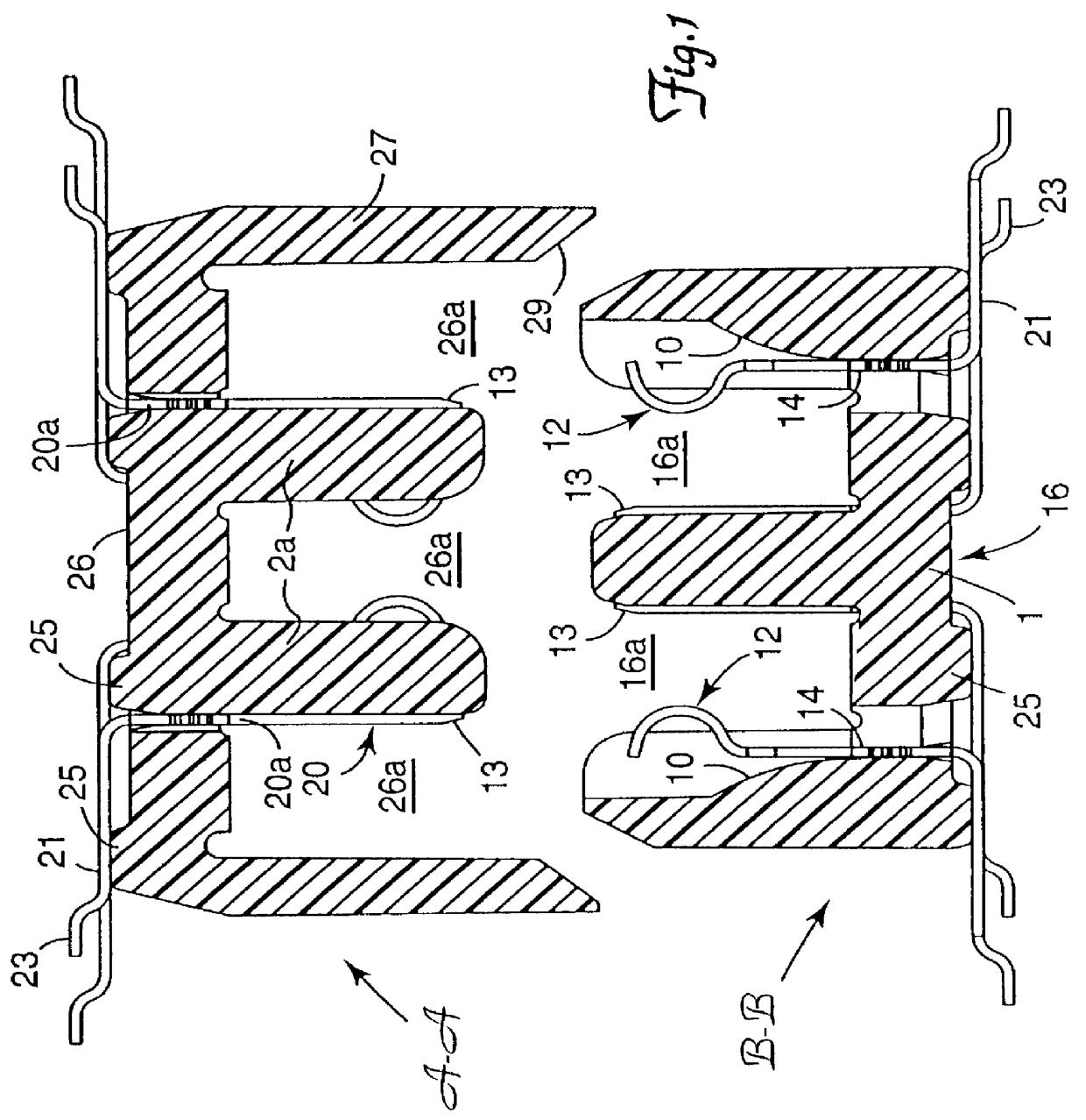
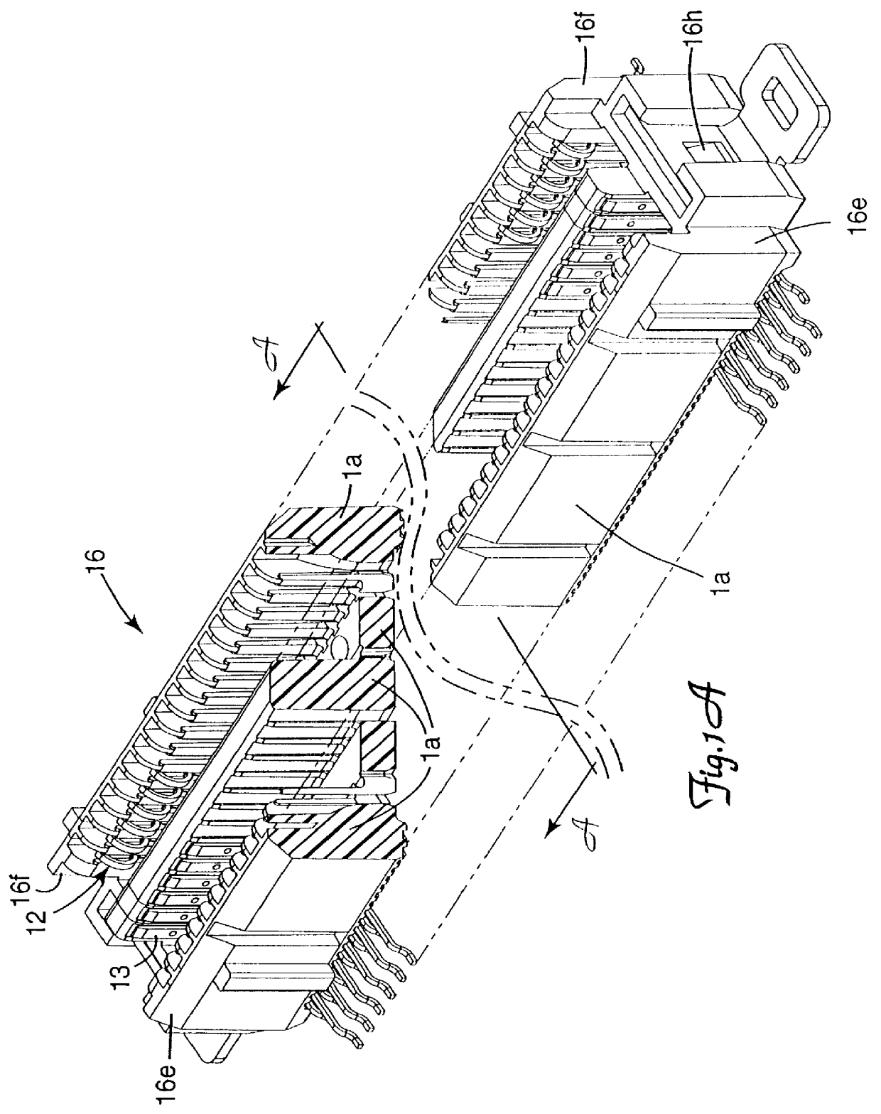
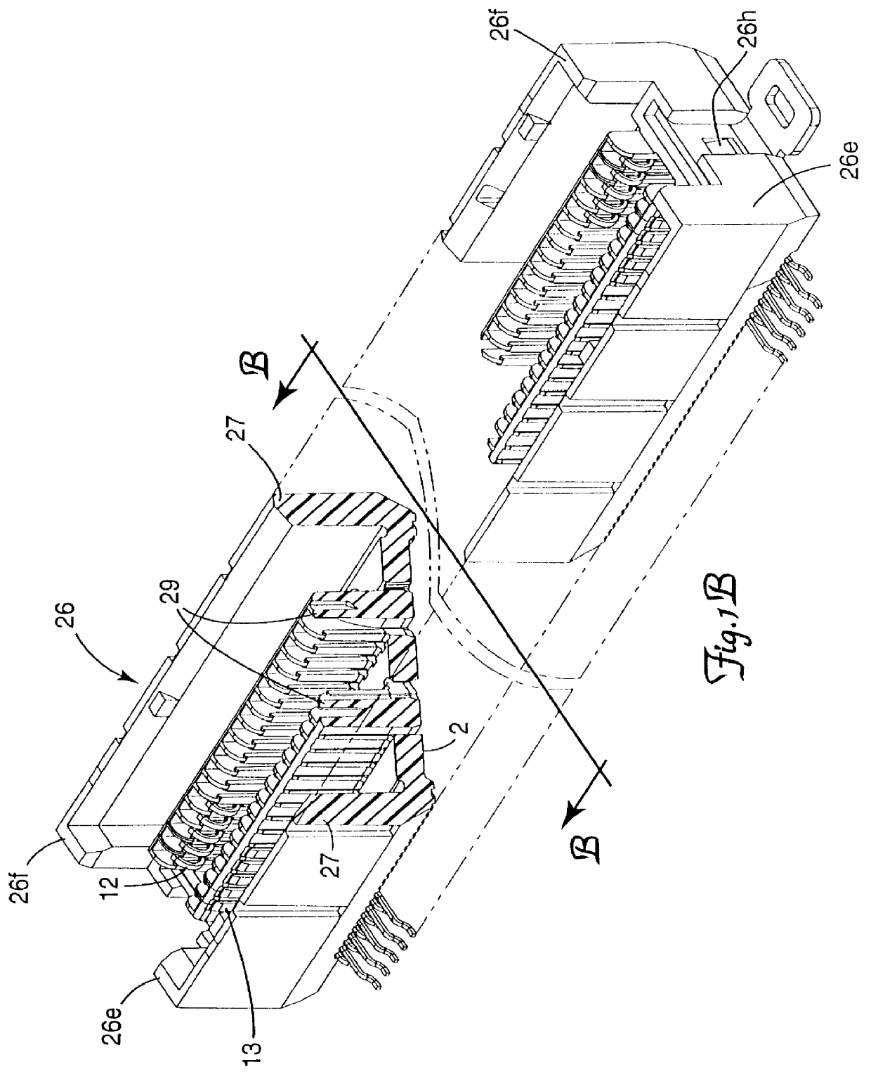
In accompanying drawing, FIGS. 88, 89 and 90 illustrate an interconnection according to the present invention similar to that shown in FIGS. 1A and 1B, comprising a socket 610 and a plug 611, each of which utilize passive contact elements 614 as illustrated in FIG. 94 and active contact elements 615 as illustrated in FIG. 95. The socket 610 has a body 616 comprising...

example 2

Example 2 is illustrated in FIG. 92 and represents a further embodiment of an interconnection according to the present invention. In this embodiment, the socket 650 and the plug 655 each have a body as described above. The socket body 651 comprises a base 652 and three parallel wall members 653, 654 and 656 positioned on one side of the base 652 forming a central wall member 653 and opposed identical side wall members 654 and 656. The central wall member 653 has opposite surfaces and the side wall members have surfaces opposed to the opposite surfaces of the central wall member 653. Electrical contact elements 660 and 661 are positioned along the opposite surfaces of the central wall member 653 forming two rows of contact elements and electrical contact elements 662 and 663 are positioned along the opposed surfaces of the side wall members 654 and 656, respectively, forming two additional rows of contact elements. The contact elements 661 and 662 are aligned transversely of the sock...


PUM


Abstract

An interconnection providing multiple electrical interconnections at a fine pitch can be formed in a pluggable and unpluggable form using multiple connector channels and rows of contact elements in each of a plug and socket. The contacts may be a mixture of active and passive contacts. Furthermore, a contact support structure may provide improve spring characteristics in the contacts. The contacts may be formed in a number of configurations including vertical staggering, alternating or offset patterns, mulit-level tail exit designs, rotated contacts, staggered or nonalign retention features and dedicated power contacts. Anchors or permanent latches, separable latches, and polarization keys may also be utilized. Alternative embodiments may include straddlemount and attachment clip embodiments.

Description

The invention relates generally to interconnection systems for use in electrical and electronic connectors, including two-piece, card edge, and wire interconnections. In particular, this invention relates to an improvement in fine pitch connectors for connecting printed circuit boards (PCB) for applications including board stacking, vertical to vertical, mother to daughter, vertical to right angle and / or straddle, and in one aspect relates to an improved connector comprising a plug and a socket each having four rows of electrical contact elements.DESCRIPTION OF THE PRIOR ARTThe art is replete with connectors for making multiple interconnections between boards, between boards and discreet wires, and between boards and flexible circuits, all of which have the goal of making the most interconnections per area of board space.For example, board to board connectors are illustrated in PCT Application WO 93 / 03513 published Feb. 18, 1993 and in U.S. Pat. No. 5,380,225 issued Jan. 10, 1995. T...

Claims


Application Information

Patent Timeline
IPC IPC(8): H01R13/428H01R13/432H01R12/71H01R13/46H01R13/627H01R13/64H01R24/00H01R107/00
CPCH01R23/7073H01R23/72H01R12/716H01R24/60H01R23/27H01R12/721H01R13/20H01R13/6471H01R13/6473Y10S439/953H01R13/28H01R12/73
Inventor POPE, RICHARD A.CHERNEY, THOMAS M.HARDCASTLE, DAVID S.
Owner 3M CO
Learn More