Dielectric waveguide of a laminated structure
a laminated structure and dielectric waveguide technology, applied in the direction of waveguides, electrical devices, coupling devices, etc., can solve the problems of strength problems and difficulty in manufacturing dielectric waveguides
- Summary
- Abstract
- Description
- Claims
- Application Information
AI Technical Summary
Benefits of technology
Problems solved by technology
Method used
Image

Examples
first embodiment
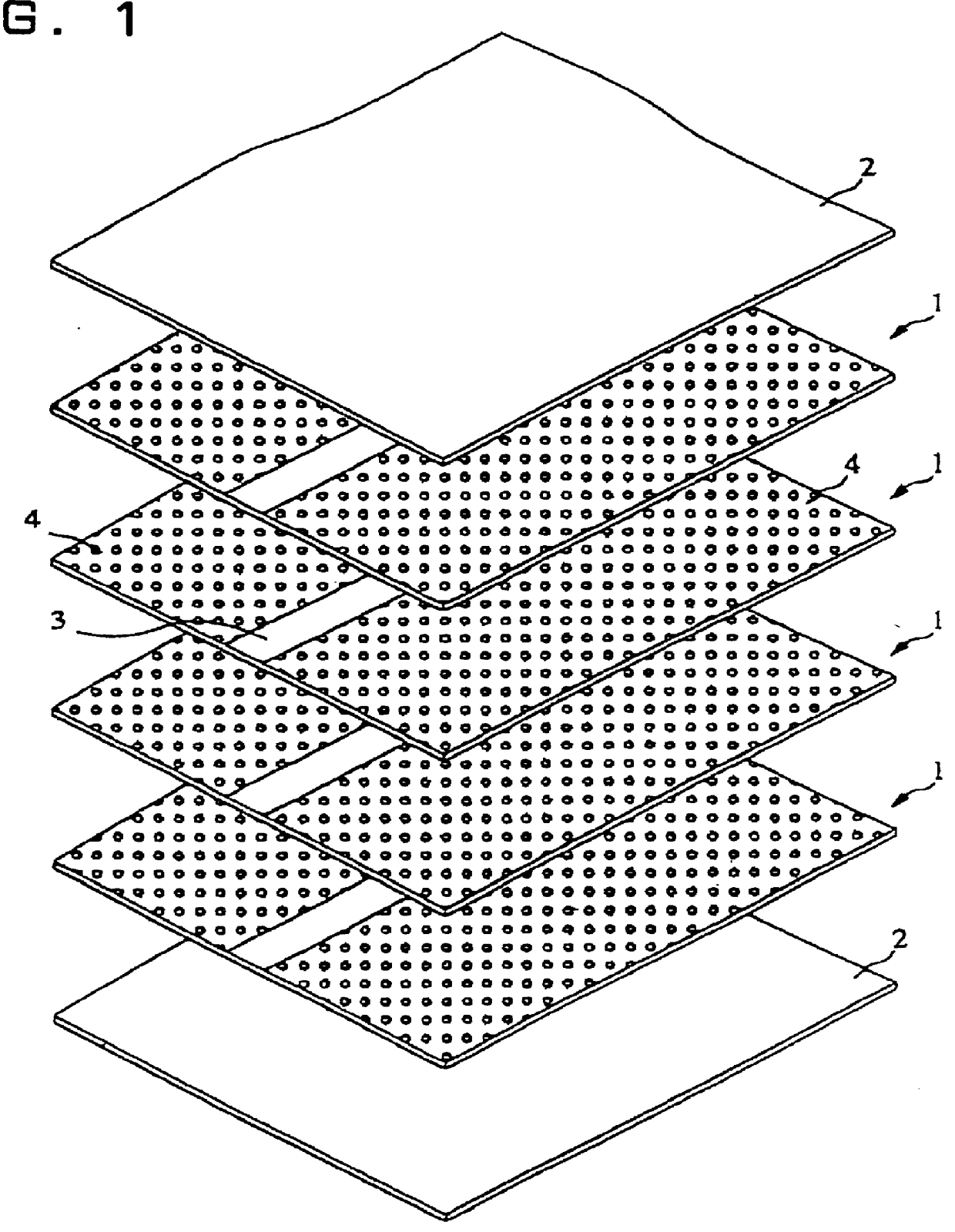
FIG. 1 and FIG. 2 show the structure of a dielectric waveguide according to the present invention.
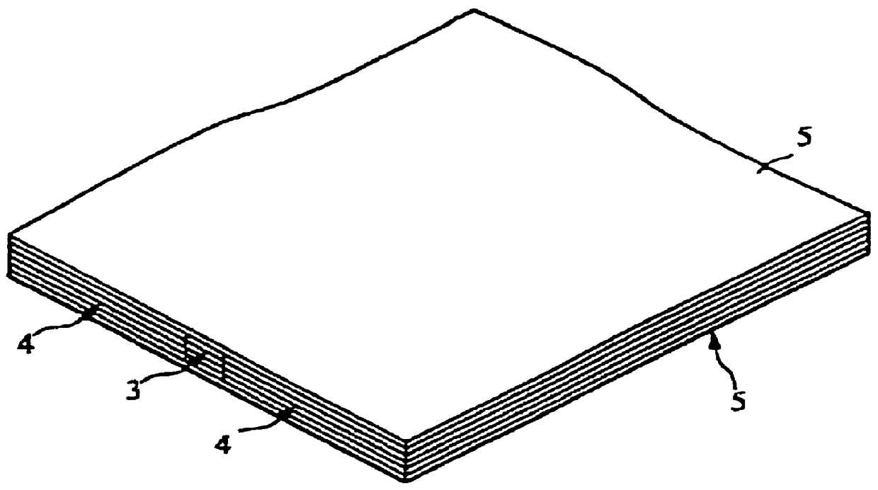
FIG. 1 is an exploded perspective view showing a plurality of separate substantially planar dielectric ceramic sheets 1,2 constituting a dielectric waveguide. The dielectric ceramic sheets 2 serving as the outermost layers have a uniform dielectric constant whereas the dielectric ceramic sheets 1 include high-dielectric-constant portions 3 and low-dielectric-constant portions 4. The low-dielectric-constant portions 4 are made by punching a number of minute holes in the dielectric ceramic sheets 1. In other words, the effective dielectric constant of the high-dielectric-constant portions 3 is the same as that of the original dielectric ceramic sheet. The effective dielectric constant of the low-dielectric-constant portions 4 is lower than that of the high-electric-constant portions 3.
Alternatively, the difference between the high and low dielectric constants may be formed by joining two ...
second embodiment
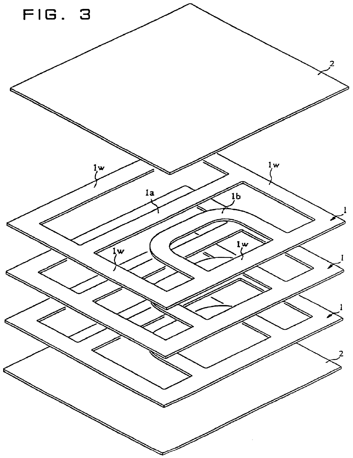
The structure of a dielectric waveguide will be described below by referring to FIG. 3 to FIG. 6.
FIG. 3 is an exploded perspective view showing the structure of a plurality of dielectric ceramic sheets in a green sheet state. In the figure, dielectric ceramic sheets 1 are provided with openings so as to define dielectric strip sections 1a and 1b which will later serve as dielectric strips, and which are connected to a frame 1w. The outermost dielectric ceramic sheets 2 are not provided with openings.
FIG. 4 is a perspective view showing the condition in which the dielectric ceramic sheets 1 and 2 illustrated in FIG. 3 have been laminated in a green sheet state and baked, and then electrode films 5 have been formed on the upper and lower surfaces thereof. After the dielectric ceramic sheets are laminated and integrated as described above, the portion enclosed by a two-dot chain line is taken off (the unnecessary portion outside the two-dot chain line is removed) to obtain a dielectri...
third embodiment
The structure of a dielectric waveguide will be described below by referring to FIG. 7 and FIG. 8.
FIG. 7 is an exploded perspective view showing the structure of a plurality of dielectric ceramic sheets in a green sheet state. In the figure, dielectric ceramic sheets 1 are provided with openings Ha and Hb. Dielectric ceramic sheets 1 and 2 are laminated and baked, electrode films are formed on both main surfaces and then an unnecessary portion is removed in the same way as shown in FIG. 4 to obtain a laminated member in which air layers are formed, for later being filled with a high-dielectric-constant dielectric.
FIG. 8 is a cross-section showing the condition in which the air layers are filled with high-dielectric-constant dielectric 7. In the figure, the high-dielectric-constant dielectric 7 has a higher relative dielectric constant than the dielectric ceramic sheets 1. In this structure, by specifying the distance between the electrode films 5, and the relative dielectric consta...
PUM
| Property | Measurement | Unit |
|---|---|---|
| dielectric constant | aaaaa | aaaaa |
| dielectric constant | aaaaa | aaaaa |
| dielectric constant | aaaaa | aaaaa |
Abstract
Description
Claims
Application Information
 - R&D
- Intellectual Property
- Life Sciences
- Materials
- Tech Scout
- Unparalleled Data Quality
- Higher Quality Content
- 60% Fewer Hallucinations
Browse by: Latest US Patents, China's latest patents, Technical Efficacy Thesaurus, Application Domain, Technology Topic, Popular Technical Reports.
© 2025 PatSnap. All rights reserved.Legal|Privacy policy|Modern Slavery Act Transparency Statement|Sitemap|About US| Contact US: help@patsnap.com