Method for making bonded metal back-plane substrates

Inactive Publication Date: 2000-05-02
IBM CORP
View PDF4 Cites 324 Cited by
  • Summary
  • Abstract
  • Description
  • Claims
  • Application Information

AI Technical Summary

Benefits of technology

Another object of the invention is to provide a conducting layer underneath the thin silicon layer that does not interfere with semiconductor manufacturing processes, is not contaminating, and can withstand processing temperatures and etching, deposition, and oxidation conditions.
In an exemplary embodiment, the present invention provides bonding at an 8-inch wafer scale with a back-plane of, for example, tungsten. Tungsten is shown to maintain its interface acuity through high temperature bonding. This allows back-plane transistors and other structures to be fabricated easily, reliably, and with excellent performance characteristics.

Problems solved by technology

A problem of conventional techniques and structures is that, at small gate lengths, it becomes increasingly difficult to control the flow of electrons by the gate and independent of the drain voltage.
Specifically, control of current close to the gated oxide / semiconductor interface is an increasingly difficult problem as gate lengths are reduced.
However, such a procedure becomes difficult at small dimensions.
Specifically, this higher doping in the substrate suffers from problems of random dopant distribution and control in placing of dopants.
However, the conventional methods of providing a back-plane for such a purpose have been problematic.
Further, large voltages are required.

Method used


Image

  • Method for making bonded metal back-plane substrates
  • Method for making bonded metal back-plane substrates
  • Method for making bonded metal back-plane substrates

Examples


first embodiment

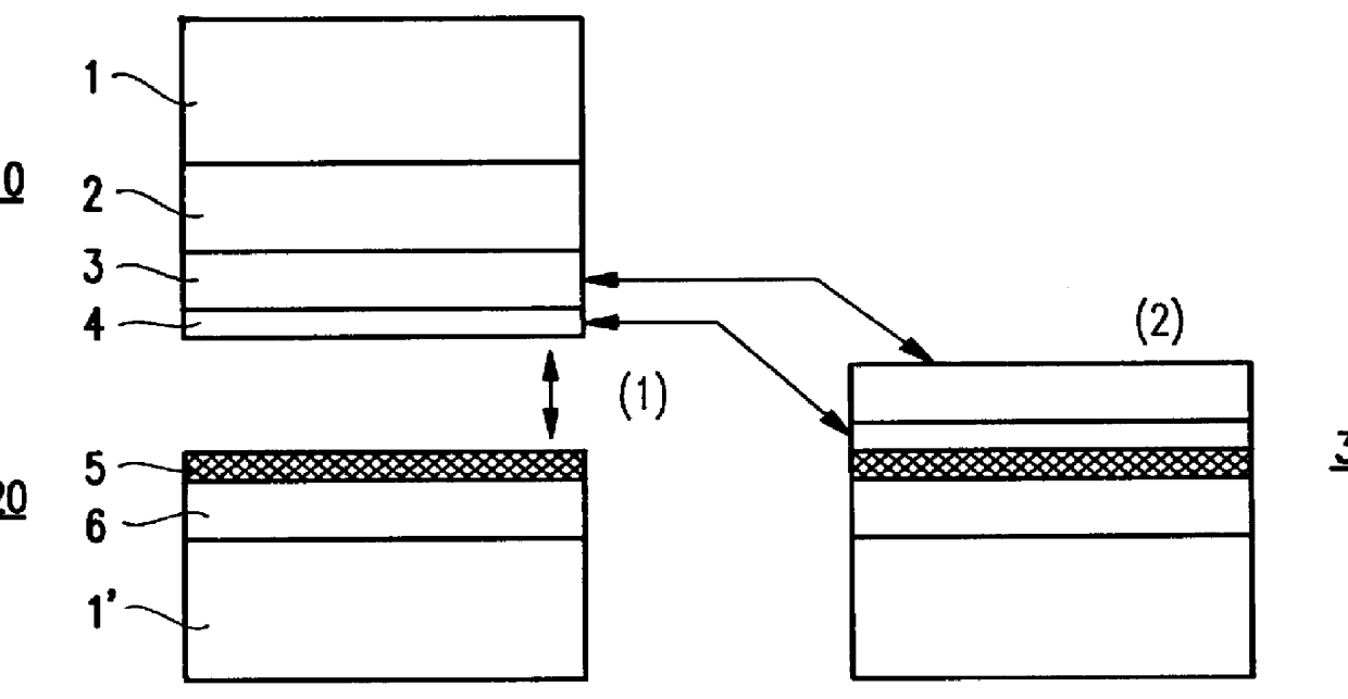
Referring now to the drawings, and more particularly to FIG. 1, there is shown the present invention.

As mentioned above, generally the present invention provides a method for attaching an insulator layer to a metal in atomically intimate contact and with negligible interface reaction. The electrical and metallurgical characteristics of the formed junction and the materials allow for fabrication of semiconducting electrical devices on them.

Turning now to FIG. 1, a preferred embodiment is shown of the method according to the present invention.

In step 1, a substrate 1 (e.g., a silicon-on-insulator (SOI) substrate 1) is provided in which an oxide layer 2 is grown on the SOI substrate 1 (e.g., a first wafer 10 forming a sacrificial wafer) where the surface roughness of the silicon starting material is kept to less than 0.5 nm in rms roughness using touch-polishing or other means. Touch-polishing is a known technique and involves orientation-selective polishing.

Preferably, the silicon-on-...

second embodiment

The second embodiment is advantageous over the first embodiment since for example the active device may be the backplane and above the back-plane may be placed the bonding device which would make it insensitive due to the bonding of oxide-oxide at the interface. However, a disadvantage would be a thicker buried oxide.


PUM


Abstract

A method of forming a semiconductor structure, includes steps of growing an oxide layer on a substrate to form a first wafer, separately forming a metal film on an oxidized substrate to form a second wafer, attaching the first and second wafers, performing a heat cycle for the first and second wafers to form a bond between the first and second wafers, and detaching a portion of the first wafer from the second wafer. Thus, a device, such as a back-plane for a semiconductor device, formed by the method includes an oxidized substrate, a metal film formed on the oxidized substrate forming a back-gate, a back-gate oxide formed on the back-gate, and a silicon layer formed on the back-gate oxide.

Description

1. Field of the InventionThe present invention generally relates to a silicon structure and to a method of making the silicon structure, and more particularly to small complementary metal oxide semiconductor (CMOS) circuitry and a method of producing the small CMOS circuitry such as transistors, memories, etc. and integration of the same using a common substrate structure.2. Description of the Related ArtBonding of silicon dioxide and silicon has been practiced for many years. Several manufacturers supply wafers in which, in a desired step, two substrates are bonded together with silicon dioxide as the bonding layers.For example, Lasky, "Wafer Bonding for Silicon-On-Insulator Technologies" Appl. Phys. Lett. 48 78(1986), described this procedure originally. Aspar et al., "Basic Mechanisms Involved in the Smart-Cut Process," Microelectronic Engineering 36 233(1997), describe the smart-cut process where a bonded wafer breaks off due to excess hydrogen. Sanchez et al., "Spontaneous Dire...

Claims


Application Information

Patent Timeline
IPC IPC(8): H01L21/70H01L21/762
CPCH01L21/76251
Inventor CHAN, KEVIN KOKD'EMIC, CHRISTOPHER PETERJONES, ERIN CATHERINESOLOMON, PAUL MICHAELTIWARI, SANDIP
Owner IBM CORP
Why Eureka
Try Eureka