
Manufacturing method of OLED panel and OLED panel

a manufacturing method and technology of organic light-emitting diodes, applied in the field of display technology, can solve the problems of increasing aperture ratio, limited capacitance, and unable to improve the aperture ratio and and achieve the effect of improving the aperture ratio and the capacitance of the oled panel

Pending Publication Date: 2022-10-06
SHENZHEN CHINA STAR OPTOELECTRONICS SEMICON DISPLAY TECH CO LTD
View PDF0 Cites 0 Cited by
  • Summary
  • Abstract
  • Description
  • Claims
  • Application Information

AI Technical Summary

Benefits of technology

The present invention is a method for making an organic light-emitting diode (OLED) panel. This method improves the aperture ratio and capacitance of the panel by overlapping a first conductive layer and a light shielding layer, and removing a pixel electrode connection in a capacitor area. This results in a high-design flexible panel that can be used for larger OLED panels and improved capacitance retention.

Problems solved by technology

Since the transparent capacitor structure does not affect a capacitor area, the aperture ratio increases, but the capacitance is limited.
Therefore, how to improve both the aperture ratio and the capacitance of the OLED panel has become a technical problem in need of solutions and research.
Conventional OLED panels have the problems of low aperture ratios and low capacitance.

Method used


Image

  • Manufacturing method of OLED panel and OLED panel
  • Manufacturing method of OLED panel and OLED panel
  • Manufacturing method of OLED panel and OLED panel

Examples


Embodiment Construction

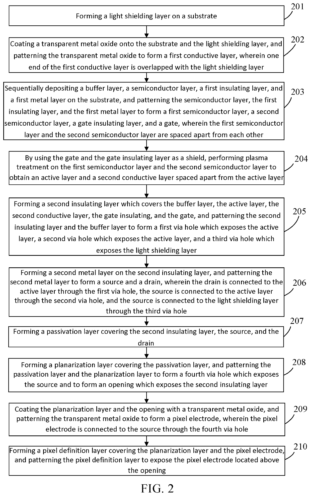
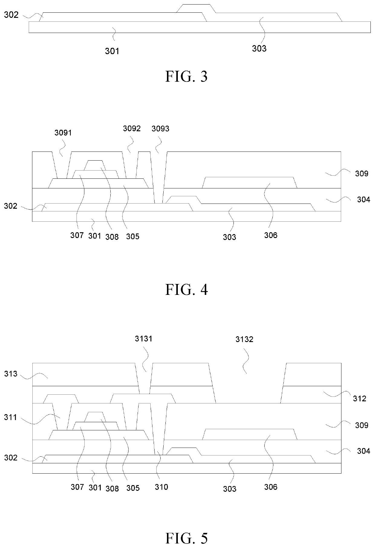
[0088]In the following, in conjunction with the accompanying drawings and with reference to the embodiments of the present application, a manufacturing method of an organic light-emitting diode (OLED) panel and the OLED panel will be clearly and completely described. Obviously, the described embodiments are only some of the embodiments of the present application, rather than all the embodiments. Based on the embodiments in the present application, all other embodiments obtained by those skilled in the art without creative work should be deemed to fall within the protection scope of the present application.

[0089]In the description of the present application, it should be understood that directional terms such as “center”, “longitudinal”, “transverse”, “length”, “width”, “thickness”, “upper”, “lower”, “front”, “rear”, “left”, “right”, “vertical”, “horizontal”, “top”, “bottom”, “inner”, and “outer” indicate orientations or positional relationship based on the drawings. The directional ...


PUM


Abstract

The present application provides a manufacturing method of an organic light-emitting diode (OLED) panel and the OLED panel. Conventional OLED panels have problems like low aperture ratios and low capacitance. The present application overlaps a first conductive layer and a light shielding layer, a pixel electrode is connected to a source, and a planarization layer and a passivation layer in a capacitor area are removed. Therefore, an aperture ratio and capacitance of the OLED panel are greatly improved, the present application has a high degree of design freedom to be used in larger-sized OLED panels, and capacitance retention is improved.

Description

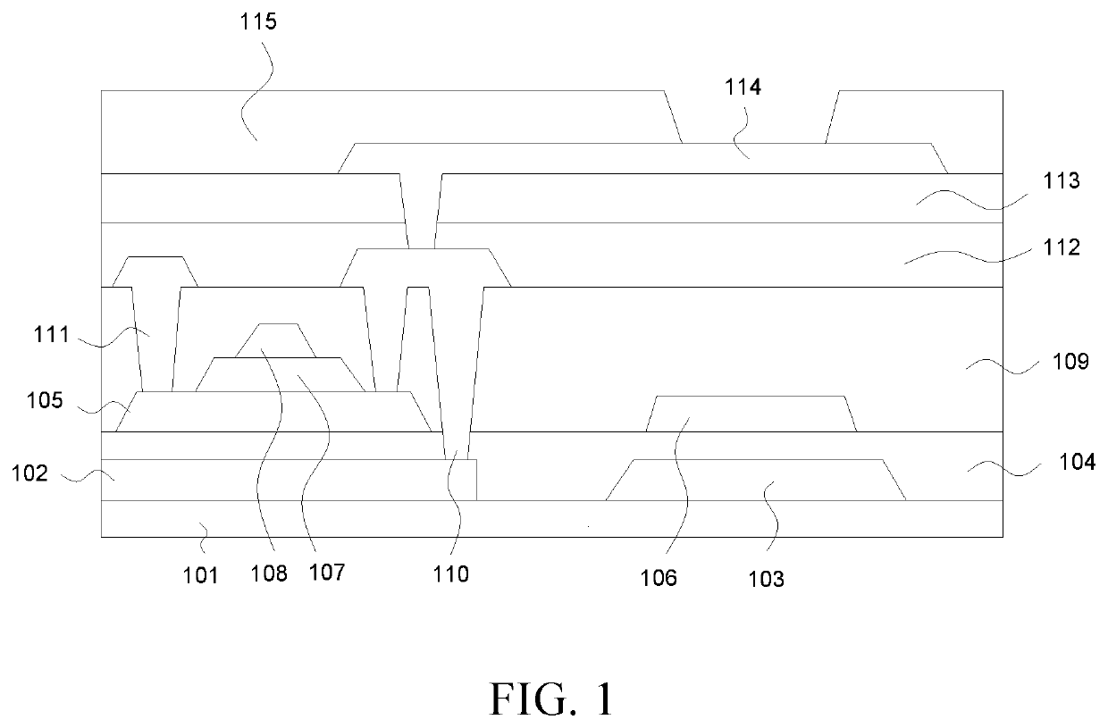
FIELD OF DISCLOSURE[0001]The present application relates to a field of display technology and in particular, to a manufacturing method of an organic light-emitting diode (OLED) panel and the OLED panel.DESCRIPTION OF RELATED ART[0002]Compared with liquid crystal displays (LCDs), the organic light-emitting devices (OLEDs) have the advantages of self-luminescence, fast response, wide viewing angles, high brightness, bright colors, being thin and light, and are considered as the next generation display technology. For a bottom-emission OLED display panel, an aperture ratio and capacitance of a capacitor are some important parameters to evaluate a product.[0003]FIG. 1 is a structural view illustrating a conventional organic light-emitting diode (OLED) panel. As shown in FIG. 1, the panel comprises a substrate 101, a light shielding layer 102, a first conductive layer 103, a buffer layer 104, an active layer 105, a second conductive layer 106, a gate insulating layer 107, a gate 108, a s...

Claims


Application Information

Patent Timeline
IPC IPC(8): H01L51/52H01L51/56H01L27/32
CPCH01L51/5284H01L51/56H01L27/3246H01L2251/306H01L2251/308H01L2227/323H10K59/122H10K59/123H10K59/124H10K59/1213H10K59/8792H10K59/126H10K2102/102H10K59/1201H10K2102/103H10K50/865H10K71/00
Inventor ZHOU, XINGYU
Owner SHENZHEN CHINA STAR OPTOELECTRONICS SEMICON DISPLAY TECH CO LTD
Learn More