
Touch display panel, manufacturing method thereof, and touch display device

a technology of touch display panel and manufacturing method, applied in the field of display technologies, can solve the problems of abnormal touch, increased risk of signal interference, and increased capacitance

Pending Publication Date: 2022-09-29
WUHAN CHINA STAR OPTOELECTRONICS SEMICON DISPLAY TECH CO LTD
View PDF4 Cites 0 Cited by
  • Summary
  • Abstract
  • Description
  • Claims
  • Application Information

AI Technical Summary

Benefits of technology

The present application provides a touch display panel with improved touch sensitivity. The touch layer includes an electrode layer and a signal conversion layer, which uses pulsed laser technology or molecular beam epitaxy to grow ferromagnetic material on the encapsulation layer. When a finger touches the touch display panel, a bioelectric signal generates a biomagnetic signal to magnetize a ferromagnetic thin-film electrode at the touch position. The Hall element converts changes in magnetic flux into changes in electrical signals, which are further converted into touch position information by the touch processing module. This results in the improvement of touch sensitivity on the touch display panel.

Problems solved by technology

However, when the flexible AMOLED has a touch requirement when bending, the sensing capacitance Cf generated by the finger touching a touch display panel is more likely to cause signal interference because the sensing capacitance Cf is smaller than the self-inductance capacitance Cb.
This causes the touch IC to fail to recognize the touch position, and touch sensitivity is low, resulting in abnormal touch.
Therefore, the current touch display panels have issues of low touch sensitivity that needs to be resolved.

Method used


Image

  • Touch display panel, manufacturing method thereof, and touch display device
  • Touch display panel, manufacturing method thereof, and touch display device
  • Touch display panel, manufacturing method thereof, and touch display device

Examples


Embodiment Construction

[0038]The descriptions of the following embodiments refer to attached drawings to illustrate specific embodiments that can be implemented in the present application. Directional terms mentioned in the present application, such as “upper”, “lower”, “front”, “back”, “left”, “right”, “inner”, “outer”, “side”, etc., just refer to directions of the attached drawings. Therefore, the directional term used is to illustrate and understand the present application, not to limit the present application. In the figure, units with similar structures are indicated by the same reference numerals.

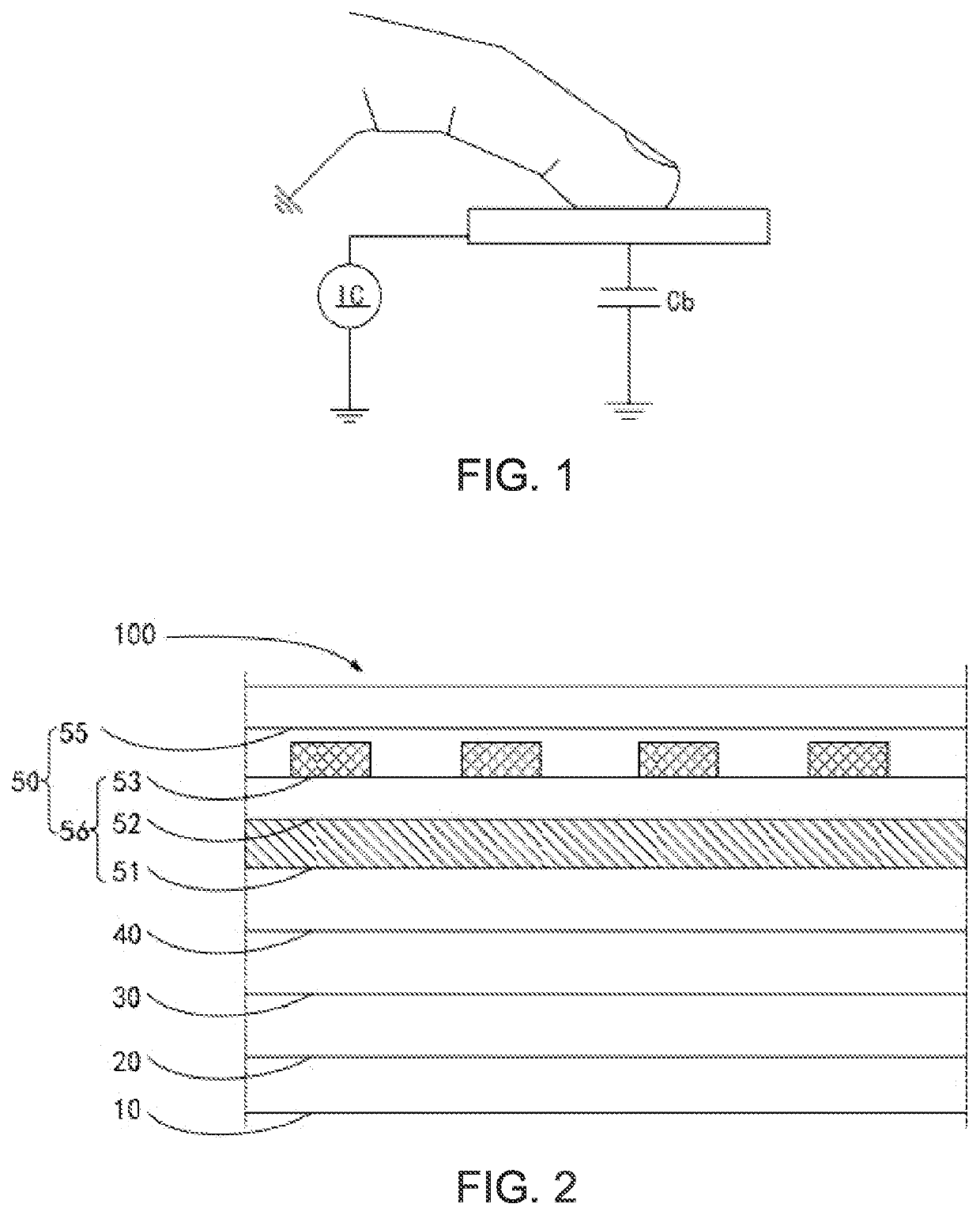
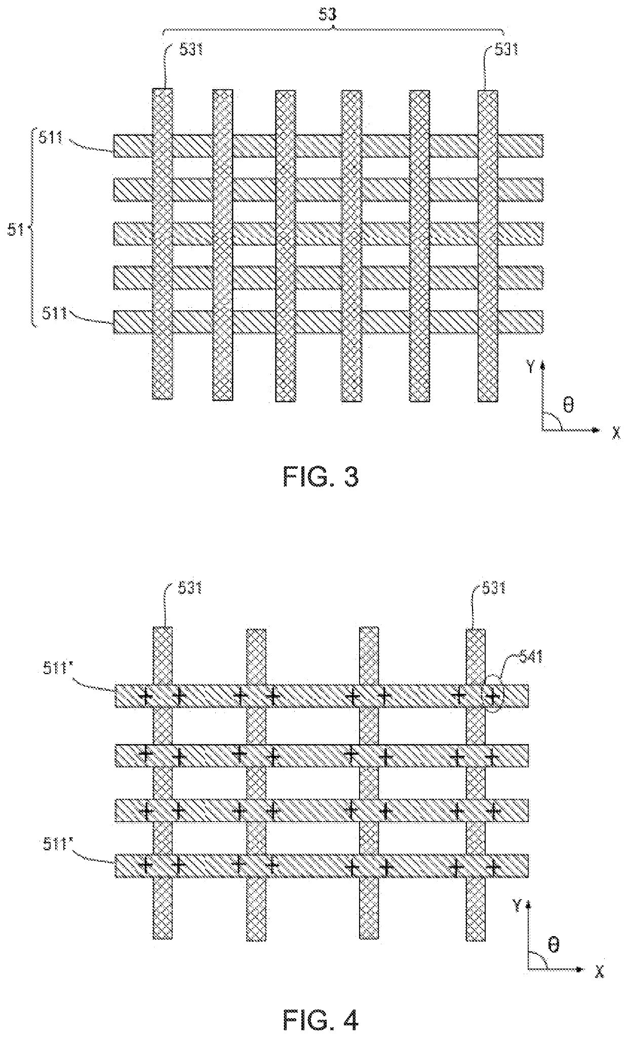
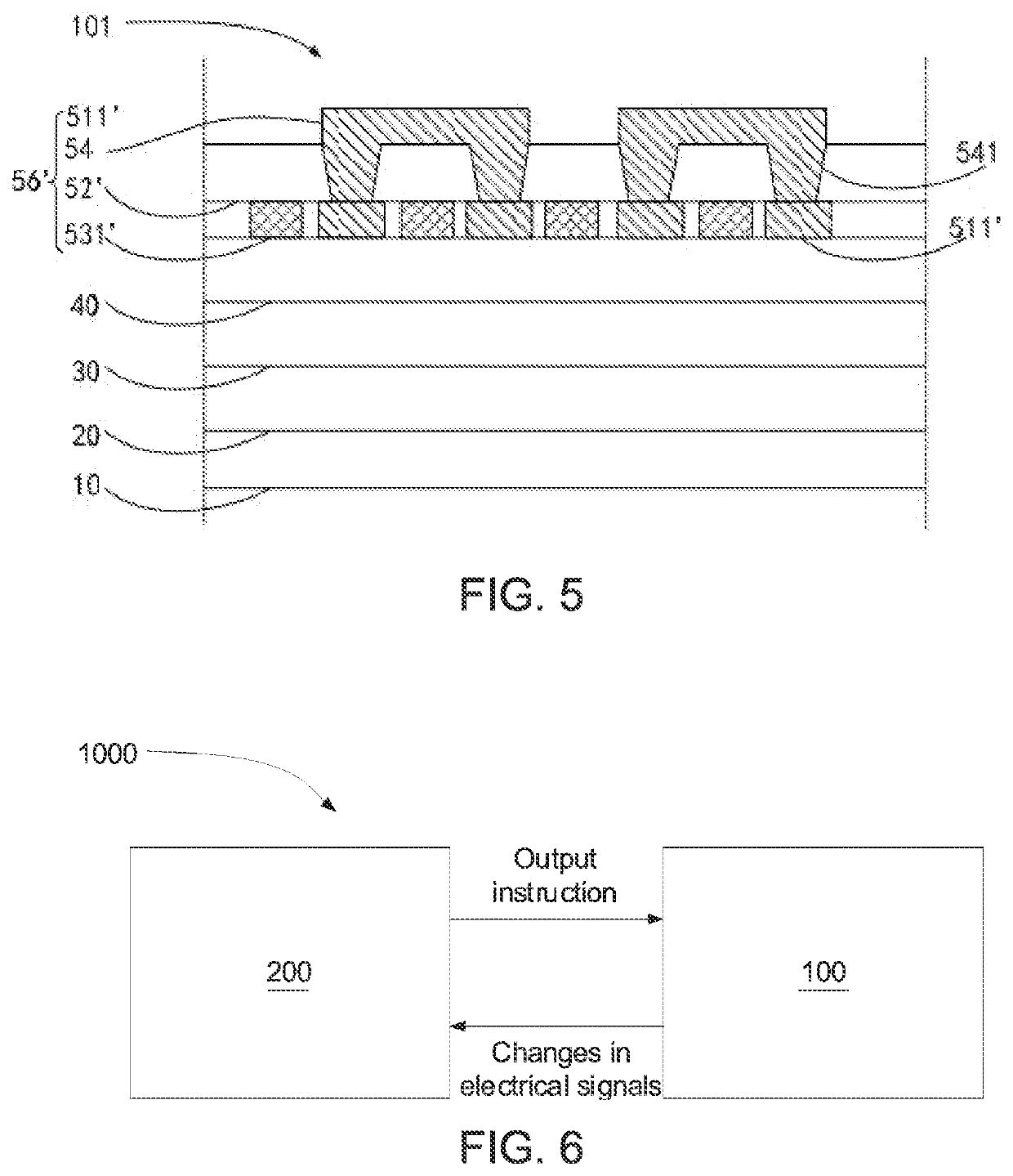
[0039]In one embodiment, as shown in FIG. 2, a touch display panel 100 is provided, which includes a substrate 10, a driving circuit layer 20, a light-emitting functional layer 30, an encapsulation layer 40, and a touch layer 50. The driving circuit layer 20 is disposed on the substrate 10. The light-emitting functional layer 30 is disposed on the driving circuit layer 20. The encapsulation layer 40 is disp...


PUM

PropertyMeasurementUnit
angleaaaaaaaaaa
angleaaaaaaaaaa
included angleaaaaaaaaaa

Abstract

A touch display panel, a manufacturing method thereof, and a touch display device are provided. The touch display panel includes a driving circuit layer, a light-emitting functional layer, an encapsulation layer, and a touch layer stacked on the substrate. The touch layer includes an electrode layer and a signal conversion layer. The electrode layer is formed by growing a ferromagnetic material on the encapsulation layer. The signal conversion layer is configured to convert a change of a magnetic signal at a touch position into an electrical signal. An interaction between a human bioelectricity and the touch layer is used to improve touch sensitivity.

Description

FIELD OF INVENTION[0001]The present application relates to the field of display technologies, and more particularly to a touch display panel, a manufacturing method thereof, and a touch display device.BACKGROUND OF INVENTION[0002]Because active matrix organic light emitting displays (AMOLEDs) have many advantages such as light, thin, unbreakable, bendable, foldable, wearable, and so on, they are often used in flexible products. Touch methods currently applied to flexible AMOLEDs in the current market are mostly capacitive touch, and because a touch layer is closer to an OLED electrode, a self-inductance capacitance of touch itself is larger. The principle of touch control is shown in FIG. 1. When a finger touches a touch screen, a sensing capacitance Cf is generated and transmitted to a touch IC. When the sensing capacitance Cf is greater than the self-inductance capacitance Cb, a position of the touch is recognized by the IC to make feedback. When the finger is away, the sensing ca...

Claims


Application Information

Patent Timeline
Patent Type & Authority Applications(United States)
IPC IPC(8): G06F3/046G06F3/041
CPCG06F3/046G06F3/0412G06F2203/04103H01L27/323G06F3/0416G06F2203/04102G06F2203/04111B32B2255/20B32B2457/208B32B2307/422B32B2255/24B32B9/04B32B2255/28B32B2307/206H10K59/40
Inventor HUANG, TIENWANGXU, JIE
Owner WUHAN CHINA STAR OPTOELECTRONICS SEMICON DISPLAY TECH CO LTD
Learn More