
Affinity sensor, in particular qcm sensor

a technology of affinity sensors and qcm, applied in the field ofaffinity sensors, can solve the problems of no prior art certainty on how nanopatterns affect the adsorption of solutes, and no situation has been reported

Pending Publication Date: 2022-09-15
LUXEMBOURG INST OF SCI & TECH LIST
View PDF5 Cites 0 Cited by
  • Summary
  • Abstract
  • Description
  • Claims
  • Application Information

AI Technical Summary

Benefits of technology

The patent describes a method for making nanoreactive materials by creating nanometer-sized doles or pores on a surface. These nanodomes and nanopores can enhance the adsorption of molecules onto the surface, resulting in higher fill factors. The method also involves creating a flat nanodome that can fill up to 60% of the surface area and forming nanopores that can reach up to 5% of the surface area. The patent shows evidence that the adsorption densities can be improved by increasing the height of the nanacafe regions, which can lead to the formation of nanoscale pillars.

Problems solved by technology

There is no certainty in the prior art on how the nanopatterns affect the adsorption of a solute.
While some authors proved an enhancement in solute adsorption on nanopatterns that went beyond what one would have expected due to the surface area, no situation has been reported where only sites, which are few orders of magnitude larger than the adsorbate species, were available for adsorption.
One important challenge in this context is to confine adsorption events within pre-determined areas down to molecular dimension.

Method used


Image

  • Affinity sensor, in particular qcm sensor
  • Affinity sensor, in particular qcm sensor
  • Affinity sensor, in particular qcm sensor

Examples


example 1

n of Gold Nanoparticles on QCM Sensor Surface

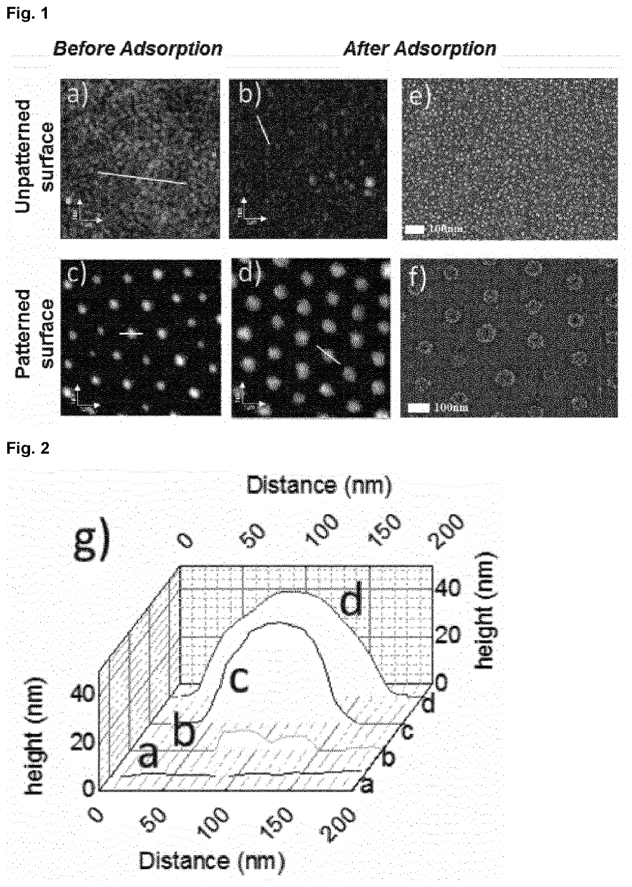
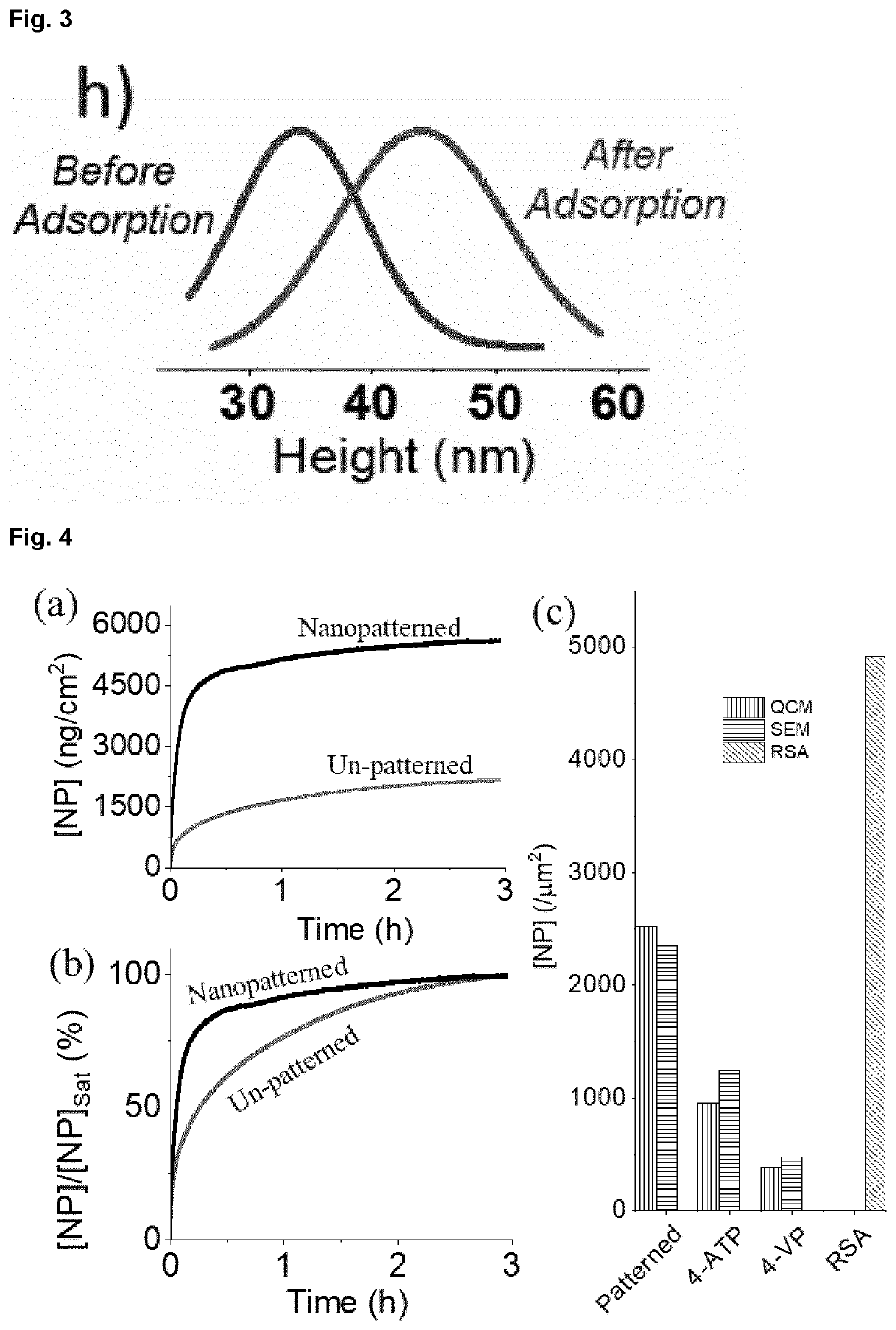
[0060]Binary nanopatterns enabling selective adsorption onto nanoscale regions may be prepared using self-assembled copolymer colloidal templates on a QCM chip surface. Details on this approach that allows creating high-density patterns of nanoscale features spanning large areas can be found, for instance in the papers by Yap, F. L.; Thoniyot, P.; Krishnan, S.; Krishnamoorthy, S. Nanoparticle, “Cluster Arrays for High-Performance SERS through Directed Self-Assembly on Flat Substrates and on Optical Fibers,” ACS Nano 2012, 6 (3), and by Nurmawati, M. H.; Ajikumar, P. K.; Renu, R.; Valiyaveettil, S., “Hierarchical Self-Organization of Nanomaterials into Two-Dimensional Arrays Using Functional Polymer Scaffold,” Adv. Funct. Mater. 2008, 18 (20), 3213-3218.

[0061]The organic copolymer templates on the surface may be converted to patterns that enable confined, selective adsorption on well-defined nanoscale features on surface. By selecting temp...

example 1a

of Gold Nanoparticles on QCM Sensor Surface Under Flow

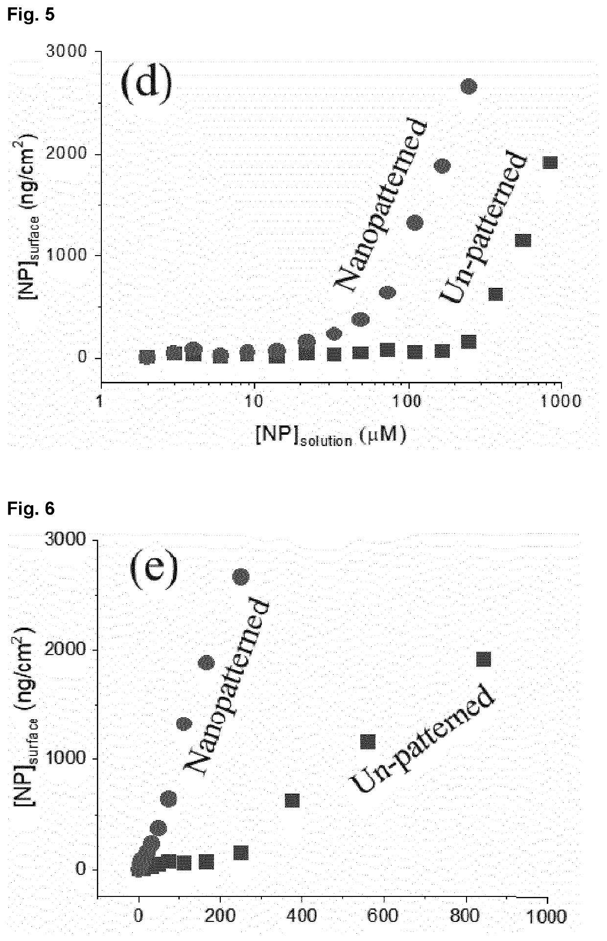
[0074]The experiments of example 1 were made in static conditions. The experiments were repeated under flow conditions. Binary patterns were prepared on QCM chips as described in example 1. The nanoscale regions with affinity for the gold nanoparticles had a surface area amounting to 33% of the total interface surface area. Gold nanoparticles were deposited from suspensions with concentrations between 85 nM and 0.85 mM. The flow of the suspensions was set to 10 μL / min (microlitres per minute), the chamber above the sensor surface had a volume of 40 μl and the temperature was held constant at room temperature. The deposition of the gold nanoparticles was monitored by QCM-D. FIG. 10 shows the deposited mass density, normalized by the surface area available for adsorption, at saturation as a function of concentration. It can be seen that significantly higher adsorption densities than on an un-patterned surface may also be obtained u...

example 1b

the Fill Factor of the Nanopattern

[0075]QCM-D measurements of the adsorption of gold nanoparticles were made as in the previous examples using nanopatterned sensor interfaces with different fill factors. The first binary pattern corresponds to the one used in examples 1 and 1a and had a fill factor of 33%. A second nanopattern had a fill factor of 61%: the nanoscale regions having affinity for the gold nanoparticles were of the same size as those of the first binary pattern but the density of the regions was increased. It was observed that the overall adsorption (taking the entire sensor interface into account) increases when the fill factor is increased. To understand if there is an influence of the fill factor on the adsorption density within the regions having affinity, the adsorbed masses were normalized by the surface area available for adsorption. No significant difference was noted, which indicates that the density of adsorbed nanoparticles within each feature remained the sa...


PUM


Abstract

An aspect of the invention pertains to an affinity biosensor for sensing an analyte (a biomolecule) in a fluid, comprising an interface for contacting the fluid and adsorption of the analyte. The interface comprises a binary pattern of nanoscale regions having affinity for the analyte and a passivated region. The nanoscale regions are isolated from one another by the passivated region in such a way that adsorption of the analyte on the interface is confined to the nanoscale regions. The nanoscale regions have diameters comprised in the range from 5 to 200 nm. The nanoscale regions have together a surface area amounting to at least 15% of the surface area of the interface. A further aspect of the invention relates to a method of using such a sensor.

Description

FIELD OF THE INVENTION[0001]The invention generally relates to affinity sensors, in particular quartz crystal microbalance (QCM) sensors. A further aspect of the invention relates to a method of sensing an analyte in a fluid using such a sensor.BACKGROUND OF THE INVENTION[0002]Confinement of adsorption processes to tiny spaces of the order of few multiples of adsorbate dimensions is encountered in sensing devices employing nanoscale components.[0003]Spatial confinement of adsorption events is a consequence of device footprint miniaturization. The outcome of the adsorption events is of interest for a broad range of applications, including nanosensors, cell-substrate interactions, antibacterial surfaces, adsorption within pores, etc.[0004]Different techniques have been used for nanopatterning of biological receptors, including colloidal lithography, block copolymer derived nanoparticle arrays, porous alumina, electron beam or nanoimprint lithography, and AFM (atomic force microscope) ...

Claims


Application Information

Patent Timeline
IPC IPC(8): G01N29/02
CPCG01N29/022G01N2291/0256B82Y15/00G01N29/222G01N2291/0426B82Y5/00
Inventor KRISHNAMOORTHY, SIVASHANKARBEGGIATO, MATTEO
Owner LUXEMBOURG INST OF SCI & TECH LIST
Learn More