Electrostatic protection element and semiconductor device

a protection element and electrostatic technology, applied in the direction of semiconductor devices, electrical devices, transistors, etc., can solve the problems of insufficient power supply damage to the esd protection transistor itself, kirk effect, etc., to prevent electrostatic reduce the susceptibility to kirk effect, and prevent damage to the internal circuit

Pending Publication Date: 2022-03-31
LAPIS SEMICON CO LTD
View PDF3 Cites 0 Cited by
  • Summary
  • Abstract
  • Description
  • Claims
  • Application Information

AI Technical Summary

Benefits of technology

The present invention relates to an electrostatic protection element and a semiconductor device that can prevent damage caused by electrostatic discharge without increasing circuit area or insuffciently powering the internal circuit. The invention achieves this by using a single MOS transistor as the electrostatic protection element, which breaks down when a high voltage due to ESD is applied, preventing current from flowing into the internal circuit. Additionally, the invention expands the current paths formed by parasitic transistors, reducing the susceptibility to the Kirk effect and suppressing a decrease in the hold voltage resulting from the Kirk effect. Thus, after the ESD ends, no large current enters the parasitic transistor even if the power source voltage is applied thereto. Overall, the invention prevents damage to both the internal circuit and the MOS transistor without increasing circuit area or insufficient power supply to the internal circuit.

Problems solved by technology

However, if the current flowing into the ESD protection transistor becomes excessively high, this can result in the Kirk effect.
Thus, there was the risk that a current based on the power source voltage would continually flow into the ESD protection transistor, resulting in insufficient power supply to the internal circuit, or damage to the ESD protection transistor itself.
However, the configuration disclosed in Japanese Patent Application Laid-Open Publication No. 2016-162844 poses the problem that because two ESD protection transistors are necessary in order to prevent damage to the ESD protection transistors along with the internal circuit, the circuit area taken up within the semiconductor device is increased.

Method used


Image

  • Electrostatic protection element and semiconductor device
  • Electrostatic protection element and semiconductor device
  • Electrostatic protection element and semiconductor device

Examples


Embodiment Construction

[0021]Embodiments of the present invention will be explained in detail below with reference to the drawings.

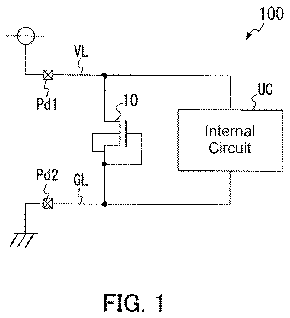
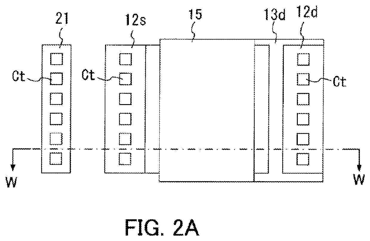
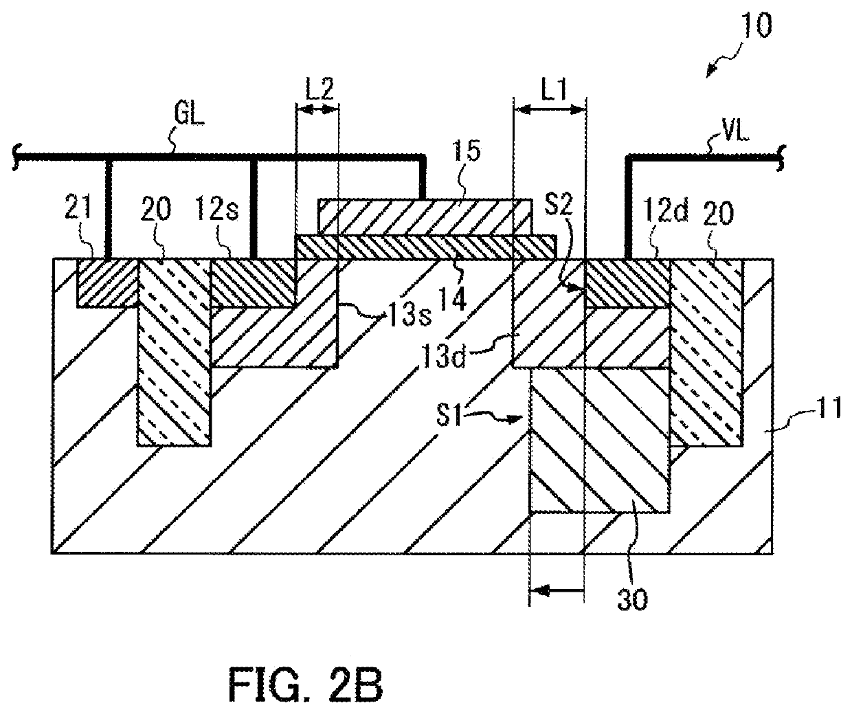
[0022]FIG. 1 is a circuit diagram that schematically shows a circuit formed in a semiconductor IC chip 100 as a semiconductor device of the present invention.

[0023]The semiconductor IC chip 100 has formed therein an internal circuit UC that performs the primary function, and an n-channel MOS (metal-oxide-semiconductor) transistor 10 as the electrostatic protection element of the present invention. Additionally, the semiconductor IC chip 100 has formed therein pads Pd1 and Pd2 that receive a power source voltage from the outside, and a power source line VL and a ground line GL that transmit the power source voltage received by the pads Pd1 and Pd2. The internal circuit UC operates using the power source voltage transmitted via the power source line VL and the ground line GL.

[0024]As shown in FIG. 1, the drain of the transistor 10 is connected to the power source line VL, and th...


PUM


Abstract

A high-density source region is formed along a surface of a semiconductor substrate and is connected to either one of a power source line and ground line. A low-density source region has an exposed surface at a surface of the semiconductor substrate and is in contact with the high-density source region. A high-density drain region is formed along the surface of the semiconductor substrate and is connected to the other one of the power source line and the ground line. A low-density drain region has an exposed surface at the surface of the semiconductor substrate, is in contact with the high-density drain region, and extends to a deeper region from the surface of the semiconductor substrate than does the low-density source region. A gate electrode is connected to either one of the power source line and the ground line.

Description

CROSS REFERENCE TO RELATED APPLICATION[0001]This application is based upon and claims the benefit of priority of the prior Japanese Patent Application No. 2020-164726, filed on Sep. 30, 2020, the entire contents of which are incorporated herein by reference.TECHNICAL FIELD[0002]The present invention relates to an electrostatic protection element and a semiconductor device including the electrostatic protection element.BACKGROUND ART[0003]Semiconductor IC chips, which are semiconductor devices, are provided with an ESD protection circuit that prevents a large current resulting from electrostatic discharge (hereinafter referred to as ESD) that occurs outside of the chip from flowing into an internal circuit via a power source terminal.[0004]The ESD protection circuit includes an ESD protection transistor that connects a power source line to a ground line if the voltage of the power source line reaches a high voltage greater than or equal to a prescribed voltage. In order to protect th...

Claims


Application Information

Patent Timeline
IPC IPC(8): H01L27/02
CPCH01L27/0274H01L27/0277
Inventor HIGASHI, MASAHIKOMOCHIZUKI, MARIE
Owner LAPIS SEMICON CO LTD
Why Eureka
Try Eureka