Semiconductor Device Signal Transmission Circuit for Drive-Control, Method of Controlling Semiconductor Device Signal Transmission Circuit for Drive-Control, Semiconductor Device, Power Conversion Device, and Electric System for Railway Vehicle

Active Publication Date: 2021-09-16
HITACHI POWER SEMICON DEVICE
View PDF5 Cites 2 Cited by
  • Summary
  • Abstract
  • Description
  • Claims
  • Application Information

AI Technical Summary

Benefits of technology

The invention provides a circuit and method for controlling signal transmission in a semiconductor device, which prevents malfunctions caused by noise and improves reliability. This results in faster switching and reduced loss of operation. The semiconductor device, power conversion device, and electric system for a railway vehicle can all benefit from this improvement.

Problems solved by technology

Since the power semiconductor module and the power semiconductor device constituting a main circuit of the power conversion device control an output current of the power conversion device, conduction loss and the switching loss occur.
However, due to the reduction in the value of the gate drive resistor, an increase in a rated output current of a gate drive circuit is required, and a damping effect by using resistive component on resonance in a path from the gate drive circuit to the power semiconductor module or the power semiconductor device is weakened, and resonance is likely to occur.
As a result, a gate portion of a semiconductor device is deteriorated or damaged, and reliability of the power semiconductor module and the power semiconductor device is reduced.
Therefore, when noise occurs, malfunction such as erroneous turn-on or parasitic vibration occurs.
At this time, when the other power semiconductor module is erroneously turned on, an arm short circuit is caused.

Method used


Image

  • Semiconductor Device Signal Transmission Circuit for Drive-Control, Method of Controlling Semiconductor Device Signal Transmission Circuit for Drive-Control, Semiconductor Device, Power Conversion Device, and Electric System for Railway Vehicle
  • Semiconductor Device Signal Transmission Circuit for Drive-Control, Method of Controlling Semiconductor Device Signal Transmission Circuit for Drive-Control, Semiconductor Device, Power Conversion Device, and Electric System for Railway Vehicle
  • Semiconductor Device Signal Transmission Circuit for Drive-Control, Method of Controlling Semiconductor Device Signal Transmission Circuit for Drive-Control, Semiconductor Device, Power Conversion Device, and Electric System for Railway Vehicle

Examples


first embodiment

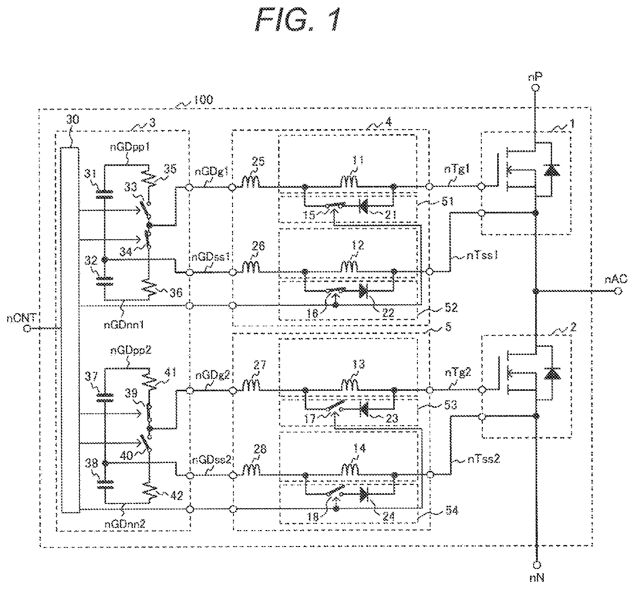
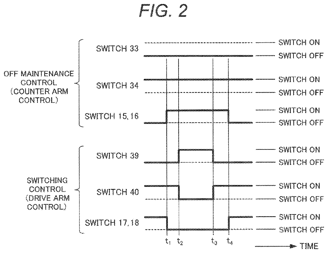
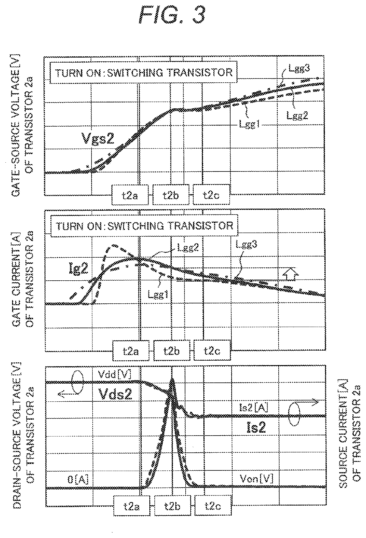
[0033]A first embodiment of the invention will be described with reference to FIGS. 1 to 6.

[0034]FIG. 1 is a circuit diagram showing a configuration of a power conversion device according to the first embodiment of the invention.

[0035]A leg circuit 100 is a component of a power conversion device, for example, a three-phase inverter for an electric railway (see FIG. 7 described later), and includes a semiconductor device, that is, power semiconductor modules 1 and 2 constituting a pair of upper and lower arms, a gate drive circuit 3 for driving the power semiconductor modules 1 and 2, and gate signal transmission circuits 4 and 5 connecting the power semiconductor modules 1 and 2 to the gate drive circuit 3. Here, each of the power semiconductor modules 1 and 2 constitutes one arm formed of a parallel connection circuit of a semiconductor switching element (MOSFET in FIG. 1) and a reflux diode.

[0036]The power semiconductor modules 1 and 2 are connected in series with each other to fo...

second embodiment

[0082]FIG. 8 is a circuit diagram showing a configuration of the power conversion device according to a second embodiment of the invention. Differences from the first embodiment will be described below.

[0083]In the second embodiment, one power semiconductor module la includes a pair of upper and lower arms. Each arm includes a parallel connection circuit of a semiconductor switching element and a reflux diode. That is, the power semiconductor module 1a is a so-called 2-in-1 type. According to such a power semiconductor module 1a, a half bridge circuit including a series connection of two arms can be configured with a short wiring distance in the module. Therefore, since a parasitic inductance (main circuit inductance) of the main circuit in the power conversion device can be reduced, a surge voltage occurred at the time of switching the switching element of the arm can be prevented. Therefore, it is possible to speed up the power semiconductor module.

[0084]The power semiconductor mo...

third embodiment

[0089]FIG. 9 is a circuit diagram showing a configuration of a power conversion device according to a third embodiment of the invention. Differences from the first embodiment will be described below.

[0090]In the third embodiment, similar to the gate signal transmission circuit in the first embodiment (FIG. 1), the gate signal transmission circuit includes inductors and impedance circuits (51 to 54) connected in parallel to the inductors. The inductor includes a series circuit of a plurality of (two in FIG. 9) inductors with a switch being connected in parallel to each inductor.

[0091]As shown in FIG. 9, in the gate signal transmission circuit 4, an inductor lla and an inductor llb are connected in series between nGDg1 and nTg1. A switch 41a and a switch 41b are connected in parallel to the inductor 11a and the inductor 11b, respectively. Further, the switch 15 for short-circuiting a series connection circuit of the inductor 11a and the inductor 11b is connected in parallel to the ser...


PUM


Abstract

To provide a semiconductor device signal transmission circuit for drive-control, a method of controlling a semiconductor device signal transmission circuit for drive-control, a semiconductor device, a power conversion device, and an electric system for a railway vehicle capable of preventing malfunction due to noise while speeding up or reducing loss of a switching operation. The semiconductor device signal transmission circuit for drive-control that is connected between a semiconductor device constituting an arm in a power conversion device and a drive circuit configured to drive the semiconductor device, including: an inductor; and an impedance circuit including a switch and connected in parallel with the inductor.

Description

CLAIM OF PRIORITY[0001]The present application claims priority from Japanese patent application JP 2020-041617 filed on Mar. 11, 2020, the content of which is hereby incorporated by reference into this application.BACKGROUND OF THE INVENTION1. Field of the Invention[0002]The present invention relates to a signal transmission circuit for drive-control that connects a semiconductor device and a drive circuit, a method of controlling the signal transmission circuit for drive-control, and a semiconductor device, a power conversion device, and an electric system for a railway vehicle that use the signal transmission circuit for drive-control.2. Description of the Related Art[0003]In devices such as industrial equipment, electric railway vehicles, hybrid vehicles, and electric vehicles, a power conversion device is widely used for power control and motor control. The power conversion device includes a power semiconductor module or power semiconductor device, a capacitor, and the like whic...

Claims


Application Information

Patent Timeline
IPC IPC(8): H03K17/16H02M1/32B60L13/00
CPCH03K17/162H02M2001/0054B60L13/006H02M1/32H02M1/08H02M1/084H02M1/088H02M7/5387H03K17/163H02M7/003H02M7/53871H02M1/0054H02M1/0064H02M1/38H02M1/0048B60L2270/147B60L2200/26B60L9/00B60L9/005
Inventor MASUDA, TORUHAYAKAWA, SEIICHITAKAYANAGI, YUJISHIMADA, TAKAEWADA, TAKASHI
Owner HITACHI POWER SEMICON DEVICE
Why Eureka
Try Eureka