
Methods for selectively forming a target film on a substrate comprising a first dielectric surface and a second metallic surface

a technology of metallic surface and target film, which is applied in the direction of basic electric elements, electrical apparatus, semiconductor/solid-state device details, etc., can solve the problems of time-consuming, expensive, and inability to meet the requirements of many applications, and achieve the effect of reducing the cost of production

Active Publication Date: 2021-05-27
ASM IP HLDG BV
View PDF0 Cites 136 Cited by
  • Summary
  • Abstract
  • Description
  • Claims
  • Application Information

AI Technical Summary

Benefits of technology

The patent text describes a new invention and its advantages compared to previous technologies. The technical effects of the invention are that certain objects and advantages are achieved, which are described in detail here. However, the invention can also be implemented in a way that optimizes certain advantages without necessarily achieving all other objects and advantages described in the patent.

Problems solved by technology

Such lithography and etch processes may be time consuming, expensive, and do not offer the precision required for many applications.
However, such processes for the formation of a target film over metallic surfaces are complex, time consuming, cost prohibitive, and will only become more complex as device feature size decreases at advanced technology nodes.

Method used


Image

  • Methods for selectively forming a target film on a substrate comprising a first dielectric surface and a second metallic surface
  • Methods for selectively forming a target film on a substrate comprising a first dielectric surface and a second metallic surface
  • Methods for selectively forming a target film on a substrate comprising a first dielectric surface and a second metallic surface

Examples


Embodiment Construction

[0015]Although certain embodiments and examples are disclosed below, it will be understood by those in the art that the invention extends beyond the specifically disclosed embodiments and / or uses of the invention and obvious modifications and equivalents thereof. Thus, it is intended that the scope of the invention disclosed should not be limited by the particular disclosed embodiments described below.

[0016]The illustrations presented herein are not meant to be actual views of any particular material, structure, or device, but are merely idealized representations that are used to describe embodiments of the disclosure.

[0017]As used herein, the term “substrate” may refer to any underlying material or materials that may be used, or upon which, a device, a circuit or a film may be formed.

[0018]As used herein, the term “metallic surface” may refer to surfaces including a metallic component, including, but not limited to, metal surfaces, metal oxide surfaces, metal silicide surfaces, met...


PUM


Abstract

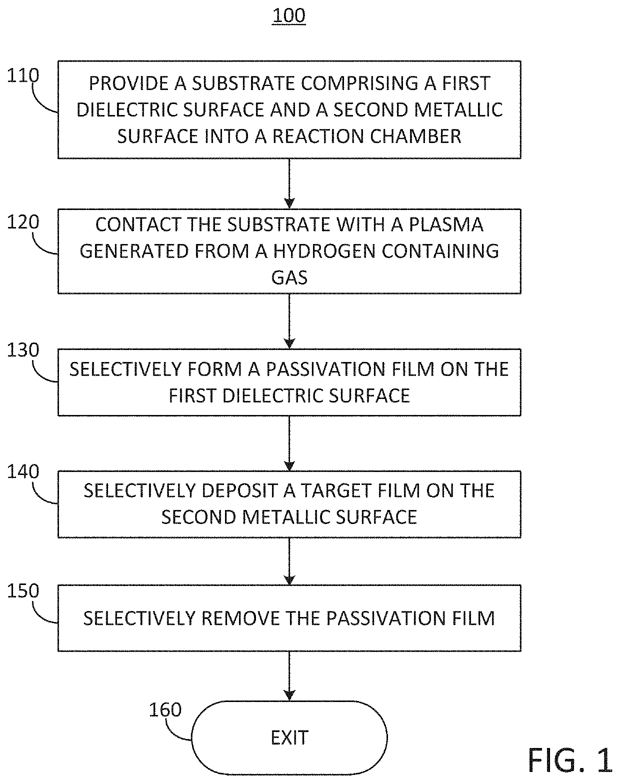
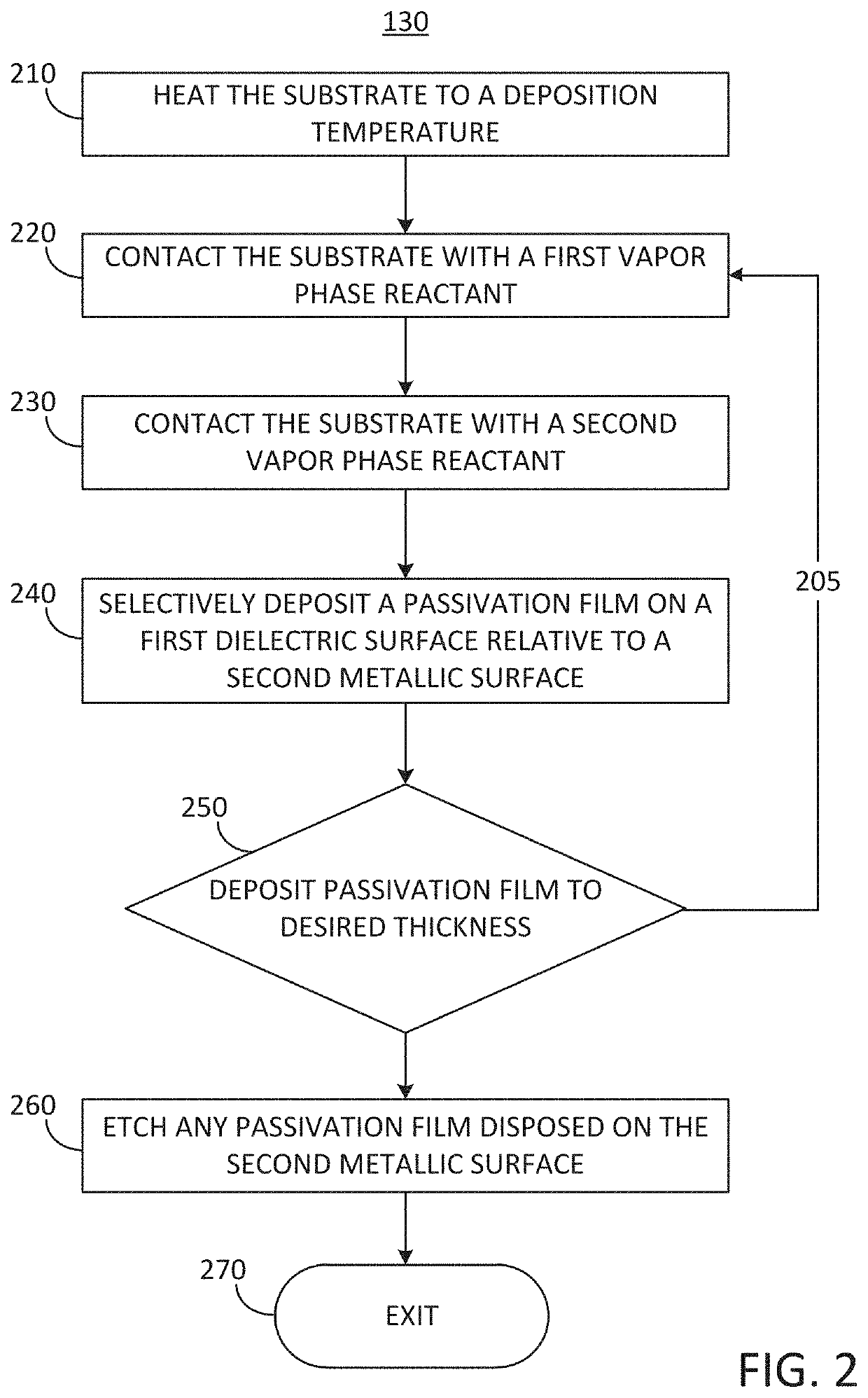
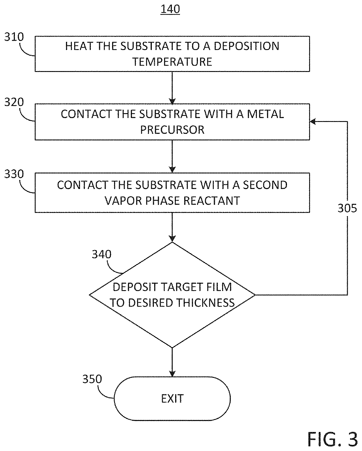
Methods for selectively forming a target film on a substrate comprising a first dielectric surface and a second metallic surface are disclosed. The methods may include: contacting the substrate with a plasma generated from a hydrogen containing gas, selectively forming a passivation film from vapor phase reactants on the first dielectric surface while leaving the second metallic surface free from the passivation film, and selectively depositing the target film from vapor phase reactants on the second metallic surface relative to the passivation film.

Description

CROSS-REFERENCE TO RELATED APPLICATIONS[0001]This application claims priority to U.S. Patent Application Ser. No. 62 / 940,705 filed Nov. 26, 2019 titled METHODS FOR SELECTIVELY FORMING A TARGET FILM ON A SUBSTRATE COMPRISING A FIRST DIELECTRIC SURFACE AND A SECOND METALLIC SURFACE, the disclosures of which are hereby incorporated by reference in their entirety.FIELD OF INVENTION[0002]The present disclosure relates generally to methods for selectively forming a target film on a substrate comprising a first dielectric surface and a second metallic surface and particularly methods for selectively forming a target film from vapor phase reactants on a second metallic surface utilizing a selectively formed passivation film.BACKGROUND OF THE DISCLOSURE[0003]In some semiconductor device fabrication processes, it may be desirable to deposit a target film only on certain areas of a substrate. Typically, such discriminating results are achieved by depositing a continuous film of the target mate...

Claims


Application Information

Patent Timeline
IPC IPC(8): H01L21/02H01L21/027H01L21/3213
CPCH01L21/02636H01L21/0273H01L21/32136H01L21/32139H01L21/0262H01L21/56H01L23/3171H01L21/02118H01L21/0228H01L21/31138H01L21/02189H01L21/32H01L21/02315H01L21/76834H01L21/02312H01L21/02271H01L21/76849H01L21/02175H01L21/28556
Inventor LONGRIE, DELPHINEDENG, SHAORENMAES, JAN WILLEM
Owner ASM IP HLDG BV
Learn More