Inertial devices with wafer-level integration of higher density proof masses and method of manufacturing

a technology of higher density and proof mass, applied in the direction of microstructural devices, acceleration measurement using interia forces, instruments, etc., can solve the problems of limited performance compared to macro-scale devices at low g acceleration and low frequency, limited market penetration of some applications, and limited application market penetration

Inactive Publication Date: 2021-05-13
SCOPRA SCI & GENIE SEC
View PDF0 Cites 1 Cited by
  • Summary
  • Abstract
  • Description
  • Claims
  • Application Information

AI Technical Summary

Benefits of technology

The patent aims to increase the number of proof masses in microelectromechanical systems (MEMS).

Problems solved by technology

They however have limited performances compared to macro-scale devices at low g accelerations and low frequencies, especially in terms of background noise and resolution.
This may have limited their market penetration for some applications such as seismology, human activity monitoring, asset tracking and structural health monitoring.
In such applications, the limitations are partly due to the small size of MEMS and the relatively low material density of their silicon proof masses.
Larger bulk micromachined silicon based devices are an explored solution, but they yield increased device footprints and thus higher costs per unit.
Gold is however expensive and has a large mismatch in coefficient of thermal expansion compared to silicon (CTE=14 vs 3).
Tungsten can also be integrated using thin film deposition, such as metal organic chemical vapor deposition (MOCVD), but this may limit the potential thickness of the masses.

Method used


Image

  • Inertial devices with wafer-level integration of higher density proof masses and method of manufacturing
  • Inertial devices with wafer-level integration of higher density proof masses and method of manufacturing
  • Inertial devices with wafer-level integration of higher density proof masses and method of manufacturing

Examples


Embodiment Construction

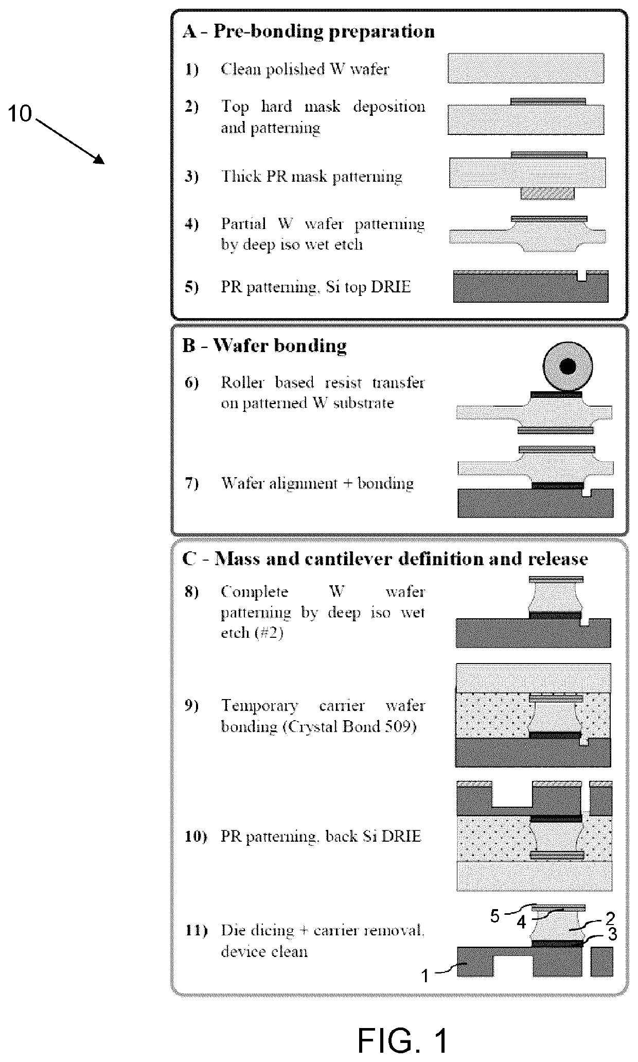
[0050]Referring to FIG. 1, there is shown a process 10 for integrating higher density proof masses with silicon at the wafer level, in accordance with an embodiment of the present disclosure. The process is used to fabricate an assembly featuring a wafer 1 with proof mass 2 or proof masses 2, as generally shown at the outset of the process. For consistency, the expression proof mass is used in the singular, but the processes described herein may have a single wafer 1 having a plurality of proof masses 2 dispersed thereon. Hence, the process, and other processes described herein may include additional steps to separate the wafer 1 with masses 2 in a plurality of inertial devices each having a portion of the wafer 1 and one or more masses 2 thereon, such as the one shown in FIG. 15 and described in further detail hereinafter. The expression “wafer” is used, but other expressions may include substrate. Moreover, the expression “assembly” is used to reference to the wafer 1 and proof ma...


PUM


Abstract

An inertial device comprises a frame. A cantilever beam has a first end connected to the frame and a second end cantilevered relative to the frame, the cantilevered beam forming a spring portion between the first end and the second end, the cantilever beam having a support surface defining a support area. The frame and the cantilever beam are made from a support wafer, the support wafer being made of silicon, a thickness of the support wafer at the support area ranging between 0 μm and 800 μm. A mass bonded to the support surface of the silicon wafer at the support area, the mass being made of tungsten, a thickness of the mass being of at least 20 μm.

Description

CROSS-REFERENCE TO RELATED APPLICATION[0001]The present application claims the priority of U.S. Provisional Patent Application No. 62 / 520,751, filed on Jun. 16, 2017 and incorporated herein by reference.TECHNICAL FIELD[0002]The present application relates to inertial devices having proof masses in microelectromechanical systems (MEMS) and to processes for manufacturing same.BACKGROUND OF THE ART[0003]Silicon-based inertial devices like microelectromechanical systems (MEMS) accelerometers and gyroscopes are now widely adopted in consumer electronic products. They however have limited performances compared to macro-scale devices at low g accelerations and low frequencies, especially in terms of background noise and resolution. This may have limited their market penetration for some applications such as seismology, human activity monitoring, asset tracking and structural health monitoring. In addition, MEMS vibration energy harvesters are considered as an emergent solution to power the...

Claims


Application Information

Patent Timeline
IPC IPC(8): G01C19/5656G01C19/5663B81B3/00
CPCG01C19/5656G01C19/5663B81B2203/0118B81B2201/0235B81B3/0018B81B2201/0242B81C1/0015G01P15/09
Inventor DOMPIERRE, ANDREFRECHETTE, LUC
Owner SCOPRA SCI & GENIE SEC
Why Eureka
Try Eureka