Composition for polishing pad and polishing pad
a technology of polishing pad and polishing pad, which is applied in the direction of lapping tools, etc., can solve the problems of affecting the processing quality of the surface of the semiconductor substrate, reducing the polishing rate, and scratches and surface defects on the semiconductor substrate, so as to achieve the appropriate level of physical properties, reduce the occurrence of defects, and high polishing rate
- Summary
- Abstract
- Description
- Claims
- Application Information
AI Technical Summary
Benefits of technology
Problems solved by technology
Method used
Image


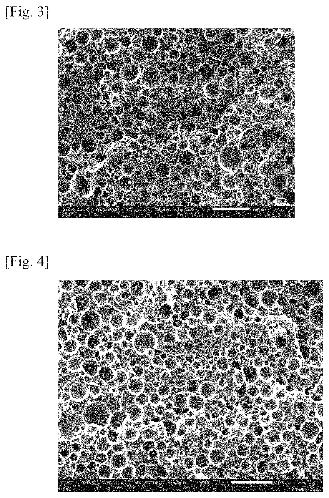

Examples
example 1
[0182]1-1: Preparation of a Urethane-Based Prepolymer
[0183]A four-necked flask was charged with toluene diisocyanate (TDI) and dicyclohexylmethane diisocyanate (H12MDI) as an isocyanate compound and polytetrarnethylene ether glycol (PTMEG) and diethylene glycol (DEG) as a polyol, followed by reaction thereof at 80° C. for 3 hours, thereby preparing a urethane-based prepolymer having a content of the NCO group of 9% by weight.
[0184]1-2: Preparation of a Polishing Pad
[0185]A casting machine equipped with tanks and feeding lines for a urethane-based prepolymer, a curing agent, an inert gas, and a foaming agent was charged with the urethane-based prepolymer prepared above. in addition, it was charged with 3,5-dimethylthio-2,6-diaminotoluene (DMTDA) as a first curing agent and 1,3-propanediol bis(l-aminobenzoate) as a second curing agent at a weight ratio of 80:20, and nitrogen gas (N2) was prepared as an inert gas. In addition, 1.18 parts by weight of a solid phase foaming agent (Akzono...
example 2
[0188]A polishing pad was prepared in the same manner as in Example 1, except that DMTDA as the first curing agent and PDPAB as the second curing agent were adjusted at a weight ratio of 60:40.
example 3
[0189]A polishing pad was prepared in the same manner as in Example 1, except that DMTDA as the first curing agent and PDPAB as the second curing agent were adjusted at a weight ratio of 50:50.
PUM
| Property | Measurement | Unit |
|---|---|---|
| weight ratio | aaaaa | aaaaa |
| elongation | aaaaa | aaaaa |
| temperature | aaaaa | aaaaa |
Abstract
Description
Claims
Application Information
 - R&D
- Intellectual Property
- Life Sciences
- Materials
- Tech Scout
- Unparalleled Data Quality
- Higher Quality Content
- 60% Fewer Hallucinations
Browse by: Latest US Patents, China's latest patents, Technical Efficacy Thesaurus, Application Domain, Technology Topic, Popular Technical Reports.
© 2025 PatSnap. All rights reserved.Legal|Privacy policy|Modern Slavery Act Transparency Statement|Sitemap|About US| Contact US: help@patsnap.com