
Display panel and organic light rmitting display panel

a display panel and organic light technology, applied in the field of display panels, can solve the problems of large parasitic capacitance of thin film transistors, inconvenient manufacturing of large-sized and high-resolution displays, etc., and achieve the effects of reducing parasitic capacitance generated between source-drain layer and gate electrode, improving display quality of corresponding display panels, and overlapping spa

Active Publication Date: 2021-01-14
HKC CORP LTD
View PDF0 Cites 0 Cited by
  • Summary
  • Abstract
  • Description
  • Claims
  • Application Information

AI Technical Summary

Benefits of technology

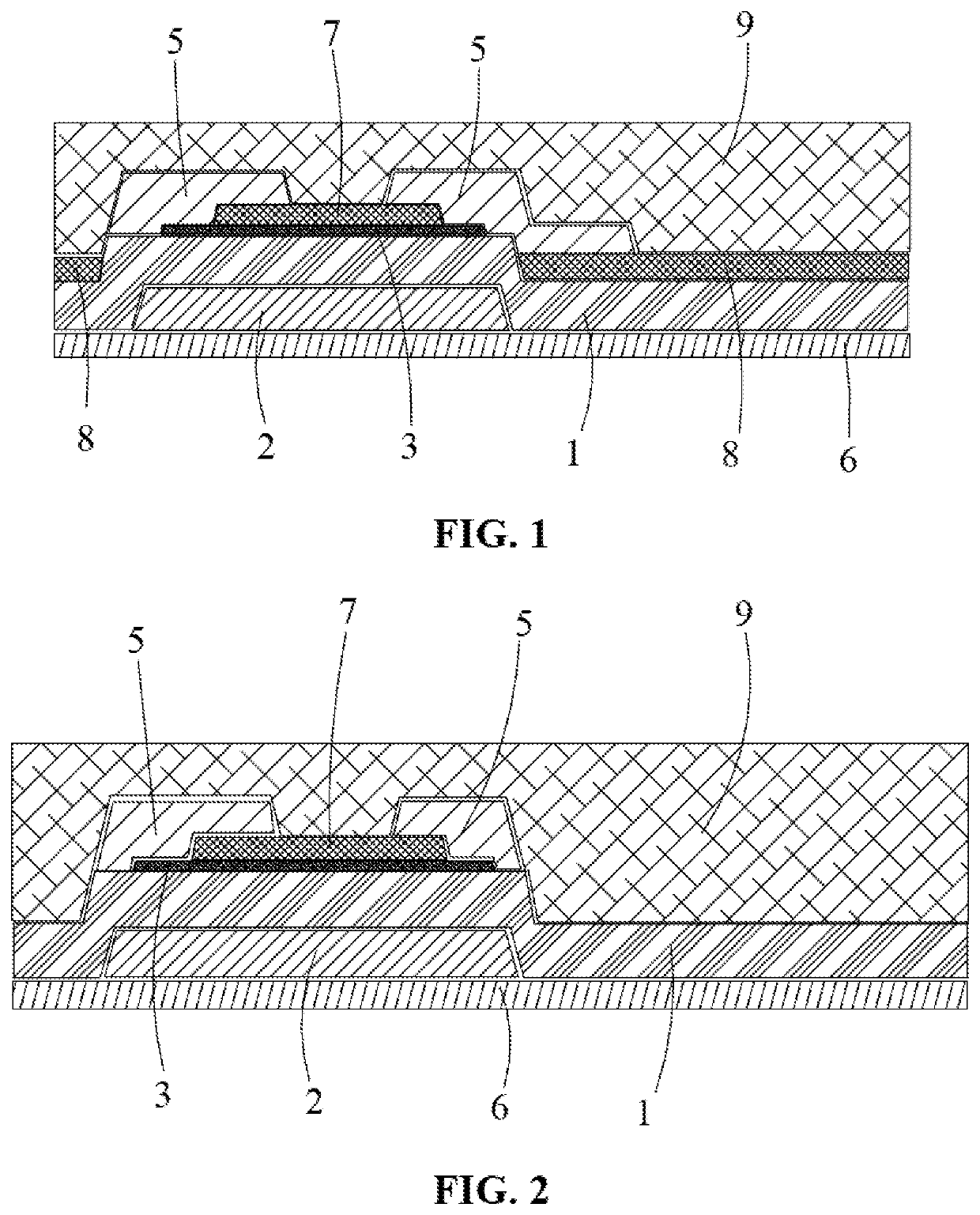
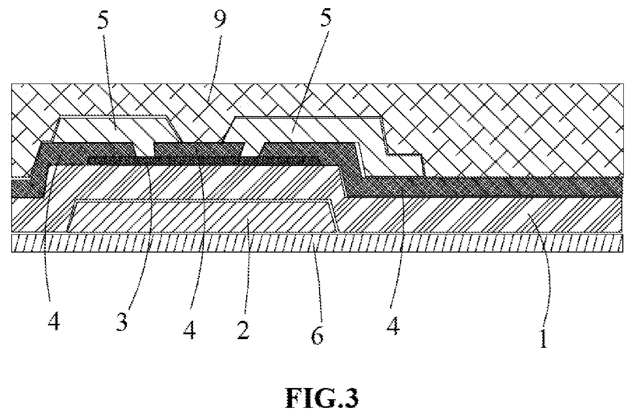
[0030]An embodiment of the present application is provided with an array substrate that the position corresponding to an edge of the semiconductor active layer and the etching barrier layer is removed, and the space between the source electrode and the drain electrode is increased, the overlapping area of the space with the gate electrode is reduced, the parasitic capacitance generated between the source-drain layer and the gate electrode is reduced, and the display quality of the corresponding display panel is improved.

Problems solved by technology

Thin film transistor (TFT) is the main functional device of the array substrate, when the TFT is manufactured, the semiconductor active layer is partially exposed by boring on the etching barrier layer, and then the source and drain electrode are partially passed through the hole etched on the barrier layer to be overlapped with a central area of the semiconductor active layer, in this way, the overlapping area between the source electrode and the drain electrode and the gate electrode under the semiconductor active layer is larger, which may cause a large parasitic capacitance of the thin film transistor, and large-sized and high-resolution display is inconvenient to be manufactured.

Method used


Image

  • Display panel and organic light rmitting display panel
  • Display panel and organic light rmitting display panel

Examples


Embodiment Construction

[0035]In order to make the purpose, the technical solution and the advantages of the present application be clearer and more understandable, the present application will be further described in detail below with reference to accompanying figures and embodiments. It should be understood that the specific embodiments described herein are merely intended to illustrate but not to limit the present application.

[0036]It is noted that when a component is referred to as being “fixed to” or “disposed at” another component, it can be directly or indirectly on another component. When a component is referred to as being “connected to” another component, it can be directly or indirectly connected to another component. Directions or location relationships indicated by terms such as “length”, “width”, “up”, “down”, “front”, “rear”, “left”, “right”, “vertical”, “horizontal”, “top”, “bottom”, “inside”, “outside”, and so on are the directions or location relationships shown in the accompanying figure...


PUM

PropertyMeasurementUnit
semiconductoraaaaaaaaaa
parasitic capacitanceaaaaaaaaaa
lengthaaaaaaaaaa

Abstract

An array substrate and a display panel; the array substrate includes a substrate (6), a gate elelctrode (2), a gate insulation layer (1), a semiconductor active layer, a first etching barrier layer (4), and a source-drain layer (5); the gate elelctrode (2) is disposed at the substrate (6); and the gate insulation layer (1) covers the gate elelctrode (2).

Description

CROSS-REFERENCE TO RELATED APPLICATIONS[0001]This application is a Divisional of U.S. patent application Ser. No. 16 / 312,746 filed on Dec. 21, 2018. This application also claims priority to Chinese Patent Application No. 201811131525.3 filed in the China Patent Office on Sep. 27, 2018, the entire content of which is incorporated herein by reference.BACKGROUND OF THE INVENTIONField of the Invention[0002]The present application relates to the field of a display panel, and more particularly to an array substrate and a display panel.Description of Related Art[0003]With the advancement of display technology, the panel display has become one of the indispensable necessaries for people. The active liquid crystal display includes an active array substrate, a color filter substrate and a liquid crystal layer located between the active array substrate and the color filter substrate. The organic light emitting diode display is mainly composed of an active array substrate and an organic light e...

Claims


Application Information

Patent Timeline
Patent Type & Authority Applications(United States)
IPC IPC(8): H01L27/12H01L27/32
CPCH01L27/1225H01L27/1248H01L27/3258H01L27/1214G02F1/1368H10K59/12H01L29/78669H01L29/78678H01L29/7869H10K59/1213H10K59/124
Inventor HUANG, BEIZHOU
Owner HKC CORP LTD
Learn More