Eureka AIR delivers breakthrough ideas for toughest innovation challenges, trusted by R&D personnel around the world.

Dense wavelength division multiplexing (DWDM) photonic integration platform

a photonic integration platform and wavelength division multiplexing technology, applied in semiconductor lasers, radioation controlled devices, instruments, etc., can solve the problems of stifling advancements towards creating fully integrated dwdm microchips and difficulties in coupling lasers

Active Publication Date: 2020-12-31
HEWLETT-PACKARD ENTERPRISE DEV LP
View PDF0 Cites 1 Cited by
  • Summary
  • Abstract
  • Description
  • Claims
  • Application Information

AI Technical Summary

Benefits of technology

The patent text describes a technology called Dense Wavelength Division Multiplexing (DWDM) that combines multiple optical signals to increase bandwidth over fiber networks. The text describes various components and methods for integrating optical sources, detectors, and other components into a photonic integrated circuit (PIC) for use in DWDM transceivers. The technical effects of the patent text include improved bandwidth and energy efficiency over electrical interconnects, as well as potential for cost savings and compact optical functions. The text also describes the use of photonic devices such as quantum dots, heterogeneous metal oxide semiconductor lasers, and athermal wavelength splitters in the PIC. The patent text also describes the process for fabricating the DWDM PIC and its components. Overall, the patent text presents a comprehensive solution for integrating optical components and methods for improving DWDM technology.

Problems solved by technology

However, there are several challenges and design considerations involved with using photonic integrated circuits (IC), which has stifled advancements towards creating fully integrated DWDM microchips.
One such challenge is associated with the integration of an optical source, such as a laser, on a photonic integrated circuit.
As an example, integrating a laser onto a silicon chip may be hampered by an indirect bandgap, which causes difficulties in coupling the laser to Silicon-On-Insulator (SOI).

Method used


Image

  • Dense wavelength division multiplexing (DWDM) photonic integration platform
  • Dense wavelength division multiplexing (DWDM) photonic integration platform
  • Dense wavelength division multiplexing (DWDM) photonic integration platform

Examples


Embodiment Construction

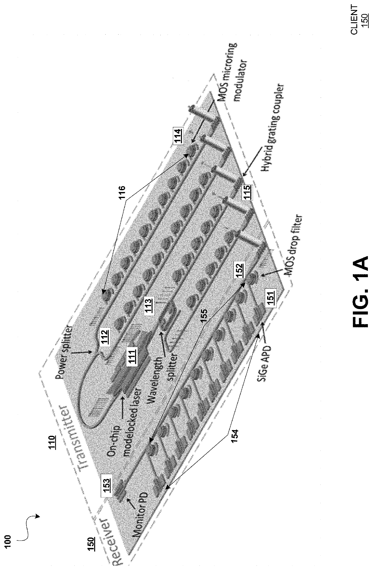
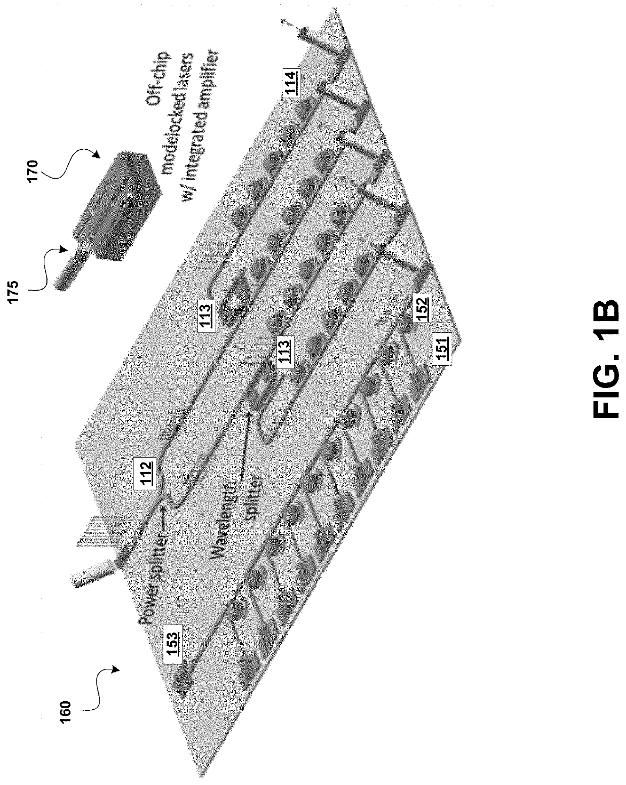
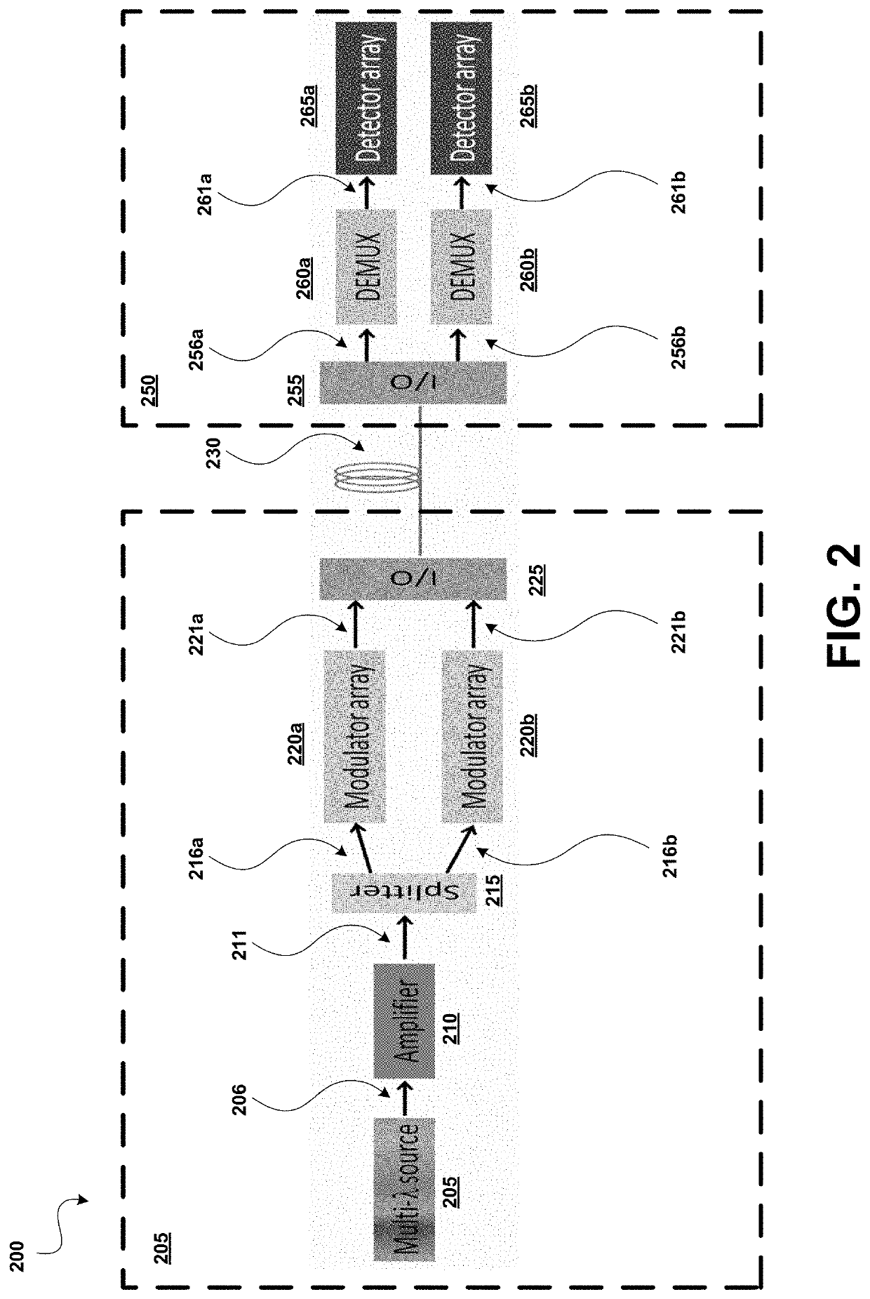
[0019]Various embodiments described herein are directed to a Dense Wavelength Division Multiplexing (DWDM) photonic integration circuit (PIC) and methods of fabricating the same. According to the embodiments, the DWDM PIC realizes the integration of multiple photonic devices on a shared platform. For example, photonic devices such as photodetectors, lasers, modulators, and the like, are often used to implement DWDM transceiver capabilities. In the DWDM PIC design, each of the photonic devices used are completely integrated on the platform, allowing these devices to be fabricated on a single integrated circuit (IC) chip (also referred to herein as “on-chip”). Moreover, in order to achieve such a high level of integration on-chip, the embodiments include methods for fabricating the DWDM PIC. As disclosed, the fabrication process includes a process that achieves bonding and layering of certain materials, such as silicon geranium (SiGe), Silicon (Si), and III-V materials in order to for...


PUM

PropertyMeasurementUnit
areaaaaaaaaaaa
structural dimensionsaaaaaaaaaa
capacitanceaaaaaaaaaa

Abstract

A Dense Wavelength Division Multiplexing (DWDM) photonic integration circuit (PIC) that implements a DWDM system, such as a transceiver, is described. The DWDM PIC architecture includes photonic devices fully integrating on a single manufacturing platform. The DWDM PIC has a multi-wavelength optical laser, a quantum dot (QD) laser with integrated heterogeneous metal oxide semiconductor (H-MOS) capacitor, integrated on-chip. The multi-wavelength optical laser can be a symmetric comb laser that generates two equal outputs of multi-wavelength light. Alternatively, the DWDM PIC can be designed to interface with a stand-alone multi-wavelength optical laser that is off-chip. In some implementations, the DWDM PIC integrates multiple optimally designed photonic devices, such as a silicon geranium (SiGe) avalanche photodetector (APD), an athermal H-MOS wavelength splitter, a QD photodetector, and a heterogenous grating coupler. Accordingly, fabricating the DWDM PIC includes a unique III-V to silicon bonding process, which is adapted for its use of SiGe APDs.

Description

CROSS REFERENCE TO RELATED APPLICATIONS[0001]This application is related to co-owned U.S. Pat. No. 9,612,503 filed on Apr. 30, 2012, entitled “HYBRID MOS OPTICAL MODULATOR”, which is hereby incorporated by reference herein in its entirety; co-pending and co-owned U.S. patent application Ser. No. 15 / 335,909 filed on Oct. 27, 2016 entitled “MULTI-WAVELENGTH SEMICONDUCTOR LASERS”, Attorney Docket No. ______, which is hereby incorporated by reference herein in its entirety; and co-pending and co-owned U.S. patent application Ser. No. ______ filed on ______, 2019 entitled “DOPED ABSORPTION DEVICES”, Attorney Docket No. ______, which is hereby incorporated by reference herein in its entirety.DESCRIPTION OF RELATED ART[0002]Dense Wavelength Division Multiplexing (DWDM) is an optical multiplexing technology used to increase bandwidth over existing fiber networks. DWDM typically consists of combining and transmitting multiple signals simultaneously, at different wavelengths, on the same fibe...

Claims


Application Information

Patent Timeline
Patent Type & Authority Applications(United States)
IPC IPC(8): G02B6/42H01S5/065H01S5/343H01S5/34G02B6/293H01L31/18H01L31/107H01L27/144H01L31/0352H01S5/02H01S5/22H01L31/0203H01L31/113H01L31/0232H01S5/30H01S5/022H01S5/026H04B10/80H04B10/40H04J14/02
CPCH01L27/1446H01S5/0215H01S5/22H01S5/343H01L31/0203H01S5/0262H04B10/801G02B6/29343H01L31/035218H04B10/40H01L31/107G02B6/29329H01S5/3009H01L31/1812H04J14/022H01L31/1133H01S5/02228H01L31/02327G02B6/4215G02B6/4286H01S5/341H01L27/1443H01S5/0657G02B6/12004G02B6/12007G02B6/34H01S5/0208H01S5/021H01S5/0265H01S5/0602H01S5/06817H01S5/1014H01S5/1032H01S5/1092H01S5/3412H01S5/02234
Inventor LIANG, DIHUANG, ZHIHONGKURCZVEIL, GEZABEAUSOLEIL, RAYMOND G.
Owner HEWLETT-PACKARD ENTERPRISE DEV LP
Why Eureka
Eureka Blog
Learn More