Semiconductor device

a technology of semiconductor devices and display devices, applied in process and machine control, program control, instruments, etc., can solve problems such as and achieve the effect of suppressing the deterioration of display devices

Active Publication Date: 2020-07-30
RENESAS ELECTRONICS CORP
View PDF0 Cites 0 Cited by
  • Summary
  • Abstract
  • Description
  • Claims
  • Application Information

AI Technical Summary

Benefits of technology

[0015]According to the semiconductor device of the present invention, it is possible to rewrite display data on the display device while suppressing a decrease in display quality of the display device.

Problems solved by technology

If the display data rewriting operation does not satisfy the specifications of the display device, the display quality of the display device may deteriorate.

Method used


Image

  • Semiconductor device
  • Semiconductor device
  • Semiconductor device

Examples


embodiment 1

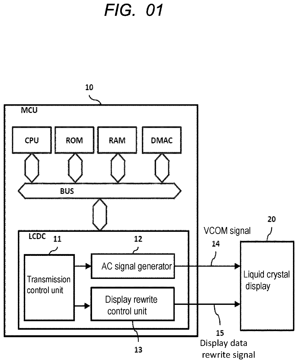
[0030]FIG. 1 is a diagram illustrating a semiconductor system according to the first embodiment. The semiconductor system 1 is an electronic device having a display panel such as an electronic timepiece, a tag device that displays product prices, and the like. The semiconductor system 1 includes a semiconductor device 10, a liquid crystal display device 20 having a display panel.

[0031]The semiconductor device 10 is a microcontroller MCU, for example, a semiconductor integrated circuit device that is formed on a semiconductor substrate such as single crystal silicon by using a CMOS transistor manufacturing method technique. The microcontroller MCU as the semiconductor device 10 includes a central processing unit CPU as a control unit, a nonvolatile memory ROM, a volatile memory RAM, a data transfer control device DMAC, a display control device LCDC, and a bus BUS. The bus BUS interconnects mutually the central processing unit CPU, the nonvolatile memory ROM, the volatile memory RAM, ...

embodiment 2

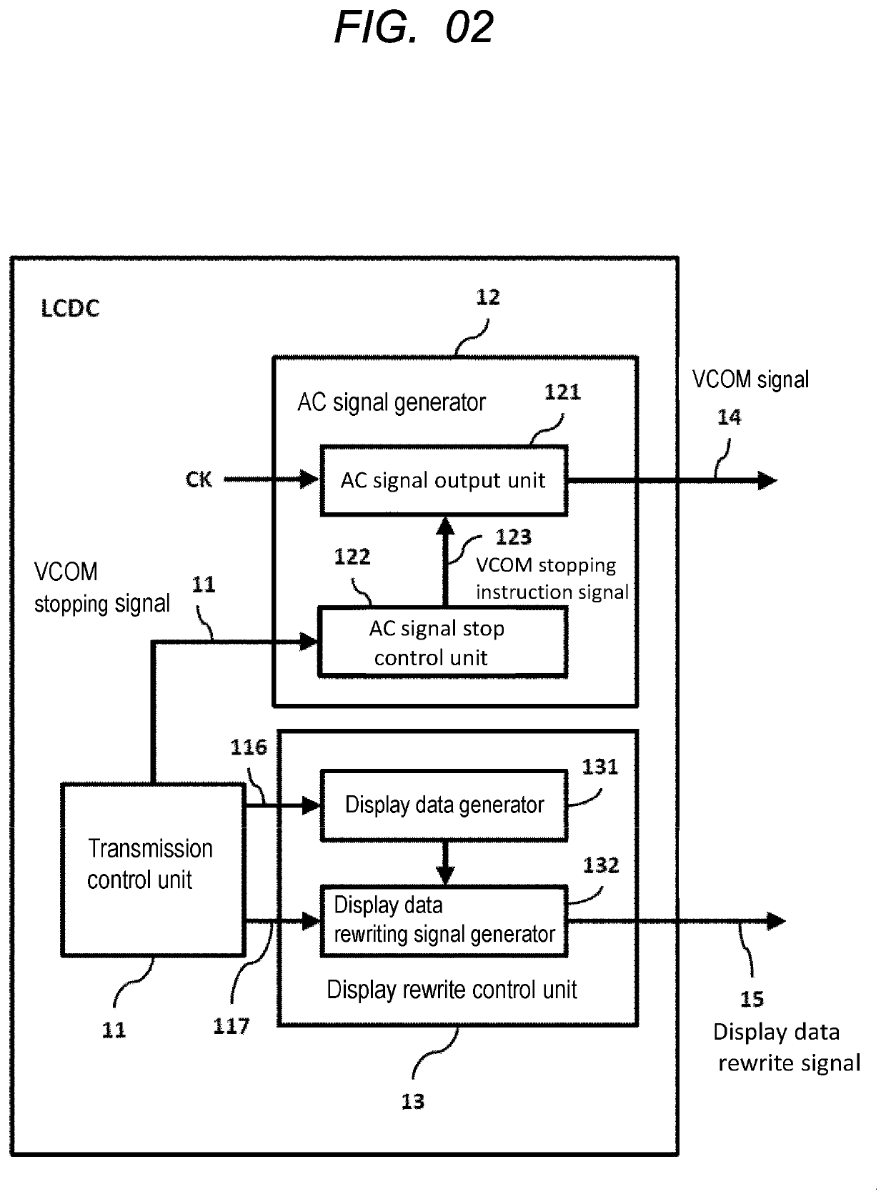
[0071]Although Embodiment 1 shows a configuration in which the change of the VCOM signal 14 is stopped by the VCOM stop signal 111 outputted from the transmission control unit 11, the present invention is not limited thereto. Embodiment 2 illustrates a configuration that allows the central processor device CPUs to halt changes in the VCOM signals 14 at any time by means of software programs executed by the CPUs.

[0072]FIG. 12 is a diagram illustrating a conceptual configuration of the semiconductor device 10 according to the Embodiment 2. In FIG. 12, the volatile memory RAM and the data-transfer control device DMACs shown in FIG. 1 are omitted. The configuration of the display control device LCDCs of FIG. 12 differs from that of FIG. 2 in that the VCOM stop signals 111 can be outputted under the control of the central processor device CPUs executing software programs in FIG. 12. Accordingly, the display control device LCDCs are provided with control registers REGs which can be set by...


PUM

PropertyMeasurementUnit
polarityaaaaaaaaaa
polarity inversionaaaaaaaaaa
polaritiesaaaaaaaaaa

Abstract

A display control device comprises an output unit that outputs an inverted polarity of an AC signal in a constant cycle, based on a signal of the constant cycle; a stop control unit that stops the reversal of the polarity of the AC signal in the output unit, based on a stop signal; a rewrite control unit for outputting a display data rewrite signal; and a transmission control unit for controlling the rewrite control unit. The stop signal stops the reversal of the polarity of the AC signal during a period in which the display data rewrite signal is output. The AC signal stopped by the stop signal maintains a polarity before the stop of polarity reversal. The output unit inverts and outputs the polarity of the AC signal, based on the signal of the constant cycle, after a period in which the display data rewrite signal is output.

Description

CROSS-REFERENCE TO RELATED APPLICATIONS[0001]The disclosure of Japanese Patent Application No. 2019-011905 filed on Jan. 28, 2019 including the specification, drawings and abstract is incorporated herein by reference in its entirety.BACKGROUND OF THE INVENTION[0002]The present disclosure relates to a semiconductor device, and more particularly, to a microcontroller or the like for controlling a displayed device.[0003]In a display device using a liquid crystal display panel, a technique is known in which a potential (VCOM potential) supplied to a common electrode of a pixel is temporally changed in order to prevent a screen burn-in (also called screen image sticking). Patent Document 1 discloses that “when the timing at which the polarity should be reversed is within the period in which the image data is output, the CPU 101 changes the timing to a timing after the period.There are disclosed techniques listed below.[0004][Patent Document 1] Japanese Unexamined Patent Application Publi...

Claims


Application Information

Patent Timeline
Patent Type & Authority Applications(United States)
IPC IPC(8): G09G3/36
CPCG09G2310/0291G09G3/3688G09G3/3614G09G2310/08G05B19/0423G05B2219/25257G09G3/3696G09G2320/0257G09G3/3685
Inventor NAGASAWA, KAZUHIRO
Owner RENESAS ELECTRONICS CORP
Why Eureka
Try Eureka