
LDPC decoder, semiconductor memory system and operating method thereof

a low density parity check and decoder technology, applied in the direction of coding, code conversion, instruments, etc., can solve the problems of finite voltage window available for threshold voltage distribution, read failure rate increase, and reliability decrease, so as to improve the performance of an ldpc decoder

Active Publication Date: 2020-07-09
SK HYNIX INC +1
View PDF0 Cites 2 Cited by
  • Summary
  • Abstract
  • Description
  • Claims
  • Application Information

AI Technical Summary

Benefits of technology

The patent is about a semiconductor memory system that can improve the performance of an LDPC decoder in an error floor region. The system has an operating method that helps to achieve this improvement. The technical effect of this patent is to enhance the efficiency and accuracy of the LDPC decoder in a memory system.

Problems solved by technology

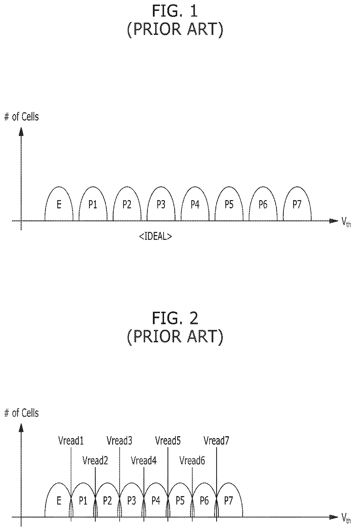
However, as the number of bits programmed in each memory cell increases, the reliability decreases and the read failure rate increases.
However, a voltage window available for threshold voltage distributions is finite.
Such charge loss may accelerate when the tunnel oxide film deteriorates by iterative program and erase operations.
The charge loss results in a decrease in the threshold voltages of memory cells.
Further, program disturbance, erase disturbance and / or back pattern dependency also cause increases in threshold voltages.
Once neighbouring threshold voltage distributions overlap, read data may include a significant number of errors when a particular read voltage is applied to a selected word line.
However, when neighbouring threshold voltage distributions overlap, a memory cell that has the third program state ‘P3’ may be erroneously determined to have the second program state ‘P2’.
In short, when the neighbouring threshold voltage distributions overlap as illustrated in FIG. 2, read data may include a significant number of errors.

Method used


Image

  • LDPC decoder, semiconductor memory system and operating method thereof
  • LDPC decoder, semiconductor memory system and operating method thereof
  • LDPC decoder, semiconductor memory system and operating method thereof

Examples


Embodiment Construction

[0046]Various embodiments are described below in more detail with reference to the accompanying drawings. The present invention may, however, be embodied in different forms and should not be construed as limited to the embodiments set forth herein. Rather, these embodiments are provided so that this disclosure is thorough and complete and fully conveys the scope of the present invention to those skilled in the art. The scope of the present invention is defined by the claims of the present invention. Also, throughout the specification, reference to “an embodiment,”“another embodiment” or the like is not necessarily to only one embodiment, and different references to any such phrase are not necessarily to the same embodiment(s).

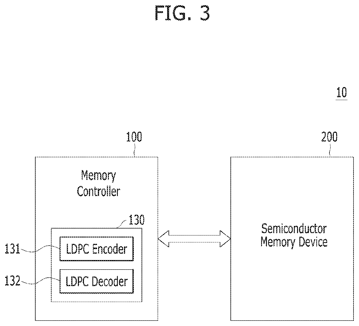
[0047]FIG. 3 is a block diagram illustrating a semiconductor memory system 10 in accordance with an embodiment of the present invention.

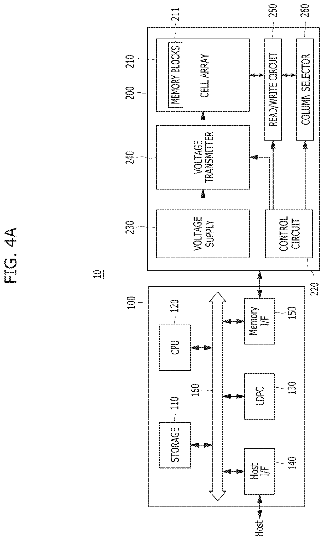
[0048]FIG. 4A is a block diagram illustrating the semiconductor memory system 10 shown in FIG. 3.

[0049]FIG. 4B is a circuit d...


PUM


Abstract

A semiconductor memory system including: a semiconductor memory device suitable for storing a codeword; and an LDPC decoder suitable for decoding the codeword to generate decoded data, wherein the LDPC decoder includes: a message passing decoding component suitable for performing a first decoding operation of decoding the codeword, and calculating the minimum value among numbers of UCNs; and an error path detection component suitable for detecting error path candidates using a tree in which each of UCNs corresponding to the minimum value is set to a root node, sorting the detected error path candidates in ascending order of maximum LLRs, resetting symbol values and LLRs of variable nodes in the error path candidates, and providing the message passing decoding unit with information on the reset symbol values and LLRs.

Description

CROSS-REFERENCE TO RELATED APPLICATION[0001]This application claims priority under 35 U.S.C. § 119 to Korean Patent Application No. 10-2019-0002635, filed on Jan. 9, 2019, which is incorporated herein by reference in its entirety.BACKGROUND1. Field[0002]Various embodiments of the present invention relate to a low density parity check (LDPC) decoder, a semiconductor memory system and an operating method thereof.2. Discussion of the Related Art[0003]In general, semiconductor memory devices are classified into volatile memory devices, such as a dynamic random access memory (DRAM) and a static RAM (SRAM), and non-volatile memory devices, such as a read only memory (ROM), a mask ROM (MROM), a programmable ROM (PROM), an erasable PROM (EPROM), an electrically EPROM (EEPROM), a ferromagnetic RAM (FRAM), a phase change RAM (PRAM), a magnetic RAM (MRAM), a resistive RAM (RRAM or ReRAM) and a flash memory.[0004]A volatile memory device loses data stored therein when power supply thereto is in...

Claims


Application Information

Patent Timeline
Patent Type & Authority Applications(United States)
IPC IPC(8): G06F11/10H03M13/11
CPCG06F11/1068H03M13/1125H03M13/1108H03M13/1111H03M13/1142H03M13/3715H03M13/6325G06F11/1012H03M13/1128G11C11/5642G11C29/52H03M13/3753
Inventor HA, JEONG-SEOKHAN, SEOK-JUOH, JI-EUN
Owner SK HYNIX INC
Learn More