Semiconductor device and method for fabricating the same

a technology of semiconductor devices and semiconductor components, applied in the direction of basic electric elements, electrical equipment, capacitors, etc., can solve the problems of deterioration in reliability of semiconductor devices, and achieve the effect of improving reliability

Active Publication Date: 2020-07-02
SK HYNIX INC
View PDF0 Cites 8 Cited by
  • Summary
  • Abstract
  • Description
  • Claims
  • Application Information

AI Technical Summary

Benefits of technology

[0004]Various embodiments of the present invention are directed to a semico...

Problems solved by technology

However, the reliability of a semiconductor device may deteriorate ...

Method used


Image

  • Semiconductor device and method for fabricating the same
  • Semiconductor device and method for fabricating the same
  • Semiconductor device and method for fabricating the same

Examples


Embodiment Construction

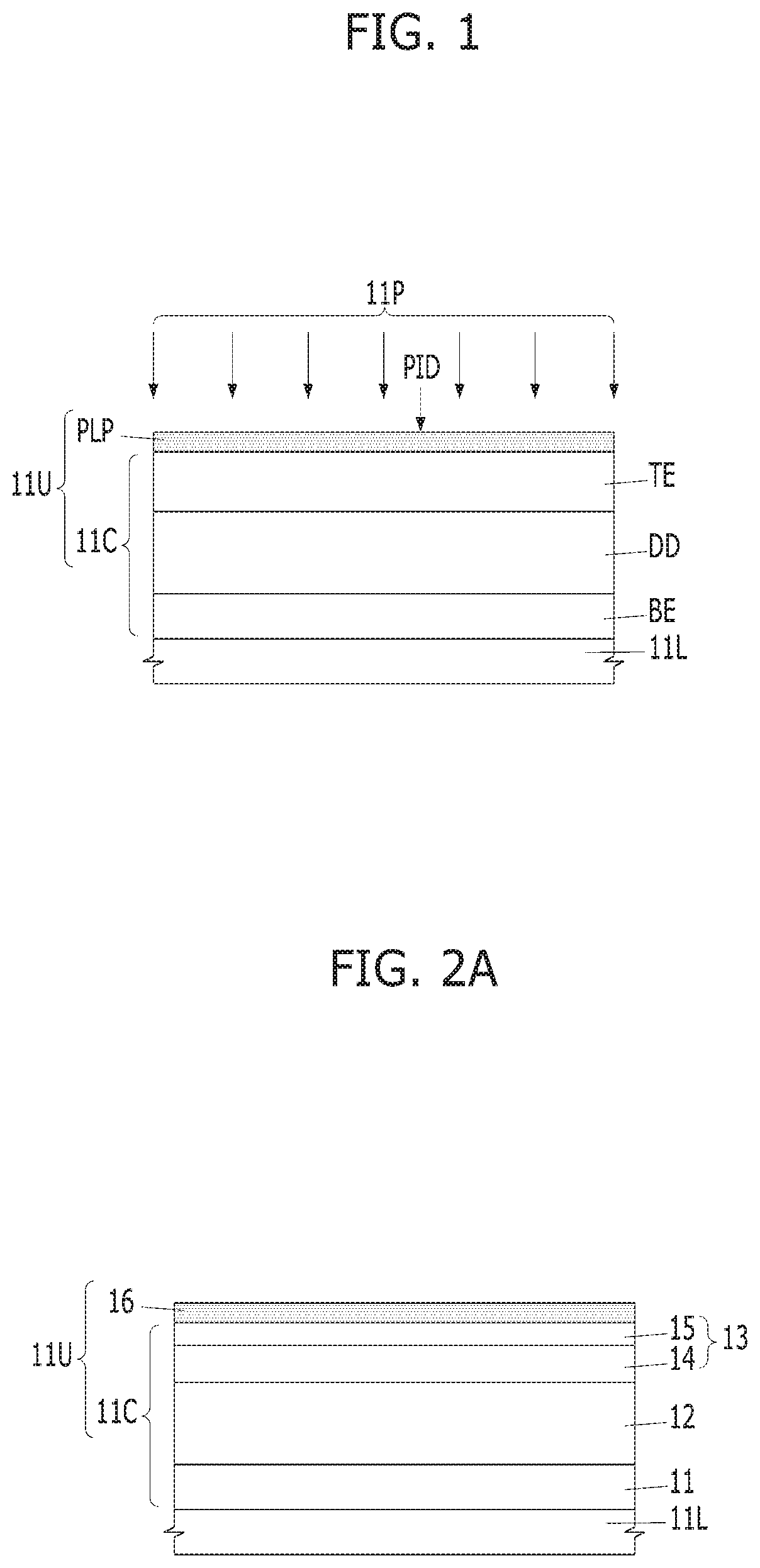
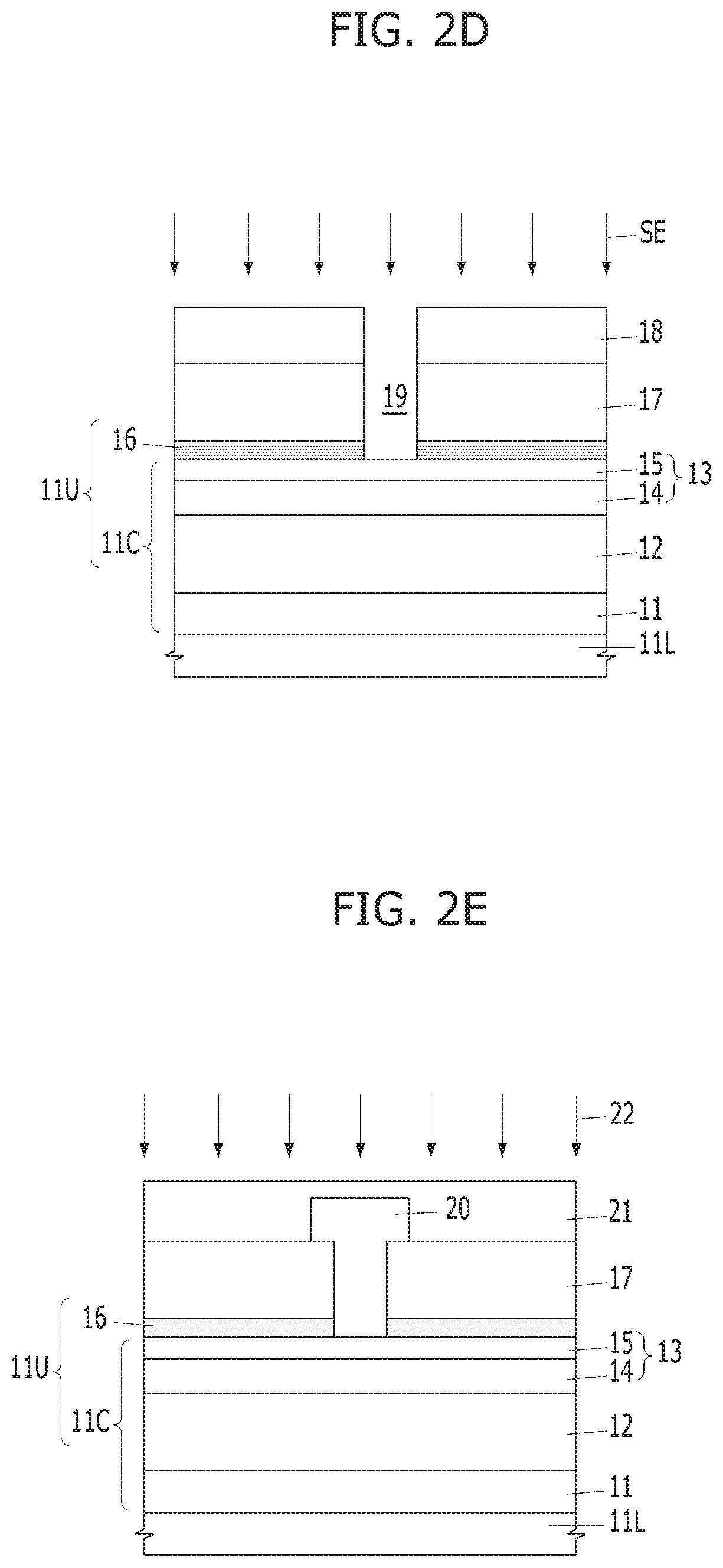
[0019]Various embodiments of the present invention will be described herein with reference to cross-sectional views, plan views and block diagrams, which are ideal schematic views of the present invention. Thus, the shape of the illustrations may be modified by fabricating techniques and / or tolerances. Accordingly, the embodiments of the present invention are not limited to the specific forms shown, but also include changes in the shapes that are generated according to the fabricating process. The regions illustrated in the figures have schematic attributes, and the shapes of the regions illustrated in the figures are intended to illustrate specific types of regions of the elements and are not intended to limit the scope of the invention.

[0020]The present invention is described herein with reference to cross-section and / or plan illustrations of idealized embodiments of the present invention. However, embodiments of the present invention should not be construed as limiting the invent...


PUM


Abstract

A method for fabricating a semiconductor device includes forming an upper structure in which a bottom electrode, a dielectric layer, a top electrode and a plasma protection layer are sequentially stacked on a lower structure, exposing the upper structure to a plasma treatment, and exposing the plasma-treated upper structure and the lower structure to a hydrogen passivation process.

Description

CROSS-REFERENCE TO RELATED APPLICATION[0001]The present application claims priority to Korean Patent Application No. 10-2018-0170952, filed on Dec. 27, 2018, which is incorporated herein by reference in its entirety.BACKGROUND1. Field[0002]Various embodiments relate generally to a semiconductor device and, more particularly, to a semiconductor device including a capacitor and a method for fabricating the same.2. Description of the Related Art[0003]Deposition and etch processes using plasma are applied in a semiconductor device fabricating process. However, the reliability of a semiconductor device may deteriorate due to a plasma induced damage which may occur during a plasma treatment.SUMMARY[0004]Various embodiments of the present invention are directed to a semiconductor device having improved reliability, and a method for fabricating the same.[0005]In accordance with an embodiment, a method for fabricating a semiconductor device may include: forming an upper structure in which a ...

Claims


Application Information

Patent Timeline
IPC IPC(8): H01L49/02
CPCH01L28/75H01L28/91H01L28/40H10B12/30H10B12/50H01L21/7687H01L21/02315H01L21/3065H01L21/31116H01L21/2257H01L21/32055
Inventor KIM, SEUNG-MUK
Owner SK HYNIX INC
Why Eureka
Try Eureka