
Electrolytic sn or sn alloy plating solution and method for producing sn or sn alloy plated article

a technology of alloy plating solution and which is applied in the field of electrolysis sn or sn alloy plating solution for forming a plated article, can solve the problems of unreachable problems, etc., and achieve the effects of preventing an influence on device malfunction, lowering pb concentration, and lowering pb concentration

Inactive Publication Date: 2020-07-02
C UYEMURA & CO LTD
View PDF0 Cites 0 Cited by
  • Summary
  • Abstract
  • Description
  • Claims
  • Application Information

AI Technical Summary

Benefits of technology

The present invention provides an electrolytic solution for plating Sn or Sn alloy with low Pb concentration. This is needed because as the semiconductor industry advances, devices become smaller, more dense, and have higher capacity, it becomes necessary to handle low alpha ray further. This solution can help in reducing the harmful effects of Pb on the environment and human health.

Problems solved by technology

Along with higher density and higher capacity of a device, an influence for malfunction of the device by an alpha ray generated from soldering material used for bonding with a semiconductor chip has become a problem which cannot be ignored.

Method used

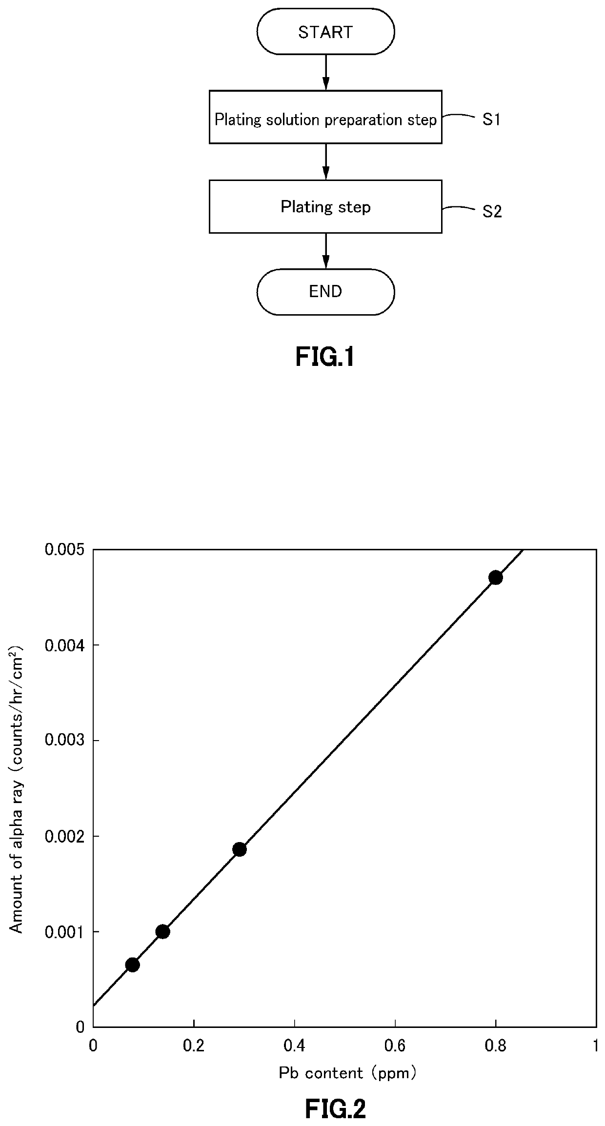

Image

  • Electrolytic sn or sn alloy plating solution and method for producing sn or sn alloy plated article
  • Electrolytic sn or sn alloy plating solution and method for producing sn or sn alloy plated article
  • Electrolytic sn or sn alloy plating solution and method for producing sn or sn alloy plated article

Examples


example 1

[0085]In an example 1, as an electrolytic Sn plating solution, a sulfur-based compound, an Sn salt, an organic acid, and a surfactant were added. As the sulfur-based compound, 5 g / L of dibenzyl disulfide was added. As the Sn salt, 40 g / L of Sn (II) alkane sulfonate was added as Sn (Sn2+). As the organic acid, 155.3 g / L, of organic sulfonic acid was added. As the surfactant, 5 g / L of polyoxyethylene alkyl phenyl ether was added. In addition, as the crystal regulator, 0.15 g / L of 2-mercapto benzothiazole was added. A solution temperature of the plating solution was 30° C., and a current density was 4 A / dm2. Further, in the example 1, a plating solution using an Sn salt with low Pb concentration of 1.0 ppm or less was also prepared.

[0086]At this time, Pb concentration in raw material metal Sn of the Sn salt was 15.454 ppm, and. Pb concentration in raw material metal Sn of the Sn salt with low Pb concentration was 0.407 ppm.

[0087]And, by using the above two plating solutions, electrolyt...

example 2

[0088]In an example 2, as the sulfur-based compound, 5 with of 4, 4′-dipyridyl disulfide was added. In addition, conditions of the Sn salt, the organic acid, the surfactant, the crystal regulator, the solution temperature, and the current density were same as the example 1.

[0089]At this time, Ph concentration in raw material metal Sn of the Sn salt was 15.454 ppm, and Pb concentration in raw material metal Sn of the Sn salt with low Pb concentration was 0.407 ppm.

[0090]And, by using the above two plating solutions, electrolytic Sn plating was performed respectively, and a eutectic ratio (%) of Pb, a eutectic amount of Pb, and a deposition potential were measured.

example 3

[0091]In an example 3, as the sulfur-based compound, 5 g / L of diphenyl disulfide was added. In addition, conditions of the Sn salt, the organic acid, the surfactant, the crystal regulator, the solution temperature, and the current density were same as the example 1.

[0092]At this time, Ph concentration in raw material metal Sn of the Sn salt was 15.454 ppm, and Pb concentration in raw material metal Sn of the Sn salt with low Pb concentration was 0.407 ppm.

[0093]And, by using the above two plating solutions, electrolytic Sn plating was performed respectively, and a eutectic ratio (%) of Pb, a eutectic amount of Pb, and a deposition potential were measured.


PUM

PropertyMeasurementUnit
water-solubleaaaaaaaaaa
concentrationaaaaaaaaaa
weight ratioaaaaaaaaaa

Abstract

The purpose of the present invention is to provide an electrolytic Sn or Sn alloy plating solution capable of lowering Pb concentration. An electrolytic Sn or Sn alloy plating solution for forming a plated article for solder bonding, at least comprising: a sulfur-based compound; an Sn salt; one or more types of acids or water-soluble salts thereof selected from inorganic acid, organic acid or water-soluble salt thereof; and a surfactant, wherein the sulfur-based compound is a thiol compound represented by following general formula (Formula. A), a salt of the thiol compound (Formula A), or a disulfide compound (Formula B).

Description

BACKGROUND OF THE INVENTIONField of the Invention[0001]The present invention relates to an electrolytic Sn or Sn alloy plating solution for forming a plated article for solder bonding and a method for producing an Sn or Sn alloy plated article for producing a plated article for solder bonding. The present application claims priority based on Japanese Patent Application No. 2017-178077 filed in Japan on Sep. 15, 2017, which is incorporated by reference herein.Description of Related Art[0002]Along with higher density and higher capacity of a device, an influence for malfunction of the device by an alpha ray generated from soldering material used for bonding with a semiconductor chip has become a problem which cannot be ignored. It is known that the alpha ray is generated mainly from Pb metal contained in the soldering material (precisely, in Sn metal) as impurities. Therefore, in the past, it is required to lower Pb concentration.[0003]For example, in Patent Literature 1, it is descri...

Claims


Application Information

Patent Timeline
Patent Type & Authority Applications(United States)
IPC IPC(8): C25D3/32C25D3/60
CPCC25D3/60C25D3/32
Inventor ENOMOTO, MASATOKANO, TOSHIKAZUOKADA, AKIRATSUJIMOTO, MASANOBUKISO, MASAYUKI
Owner C UYEMURA & CO LTD
Learn More