
Non-volatile memory and manufacturing method for the same

a manufacturing method and non-volatile memory technology, applied in the field of semiconductors, can solve the problems of large memory cell size, leakage current generation in the read operation of the cell, and the non-volatile memory cell of the single-transistor stack gate structure always has problems, so as to improve erase efficiency, enhance the effect of fn tunneling effect and increase the thickness of the tunneling dielectric layer

Active Publication Date: 2020-05-14
NEXCHIP SEMICON CO LTD
View PDF5 Cites 5 Cited by
  • Summary
  • Abstract
  • Description
  • Claims
  • Application Information

AI Technical Summary

Benefits of technology

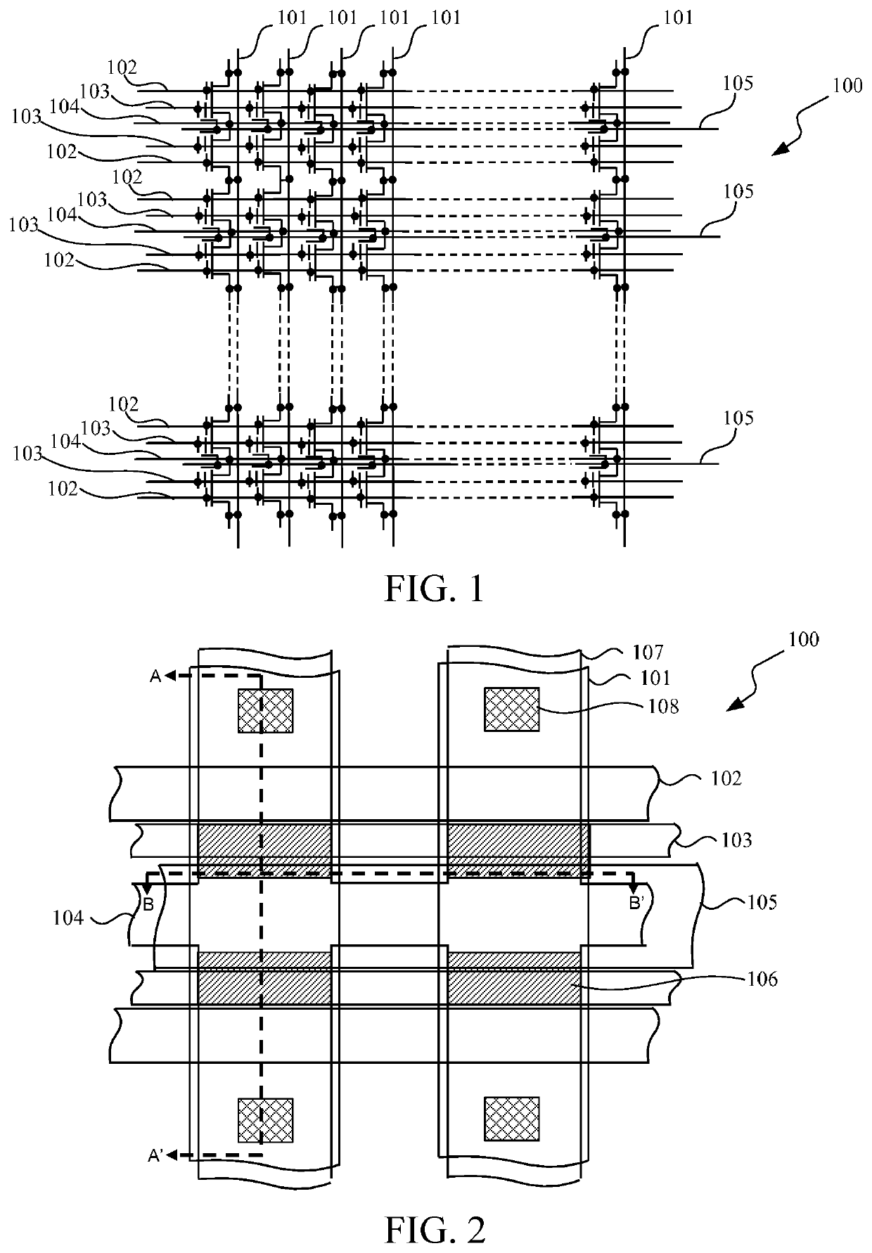
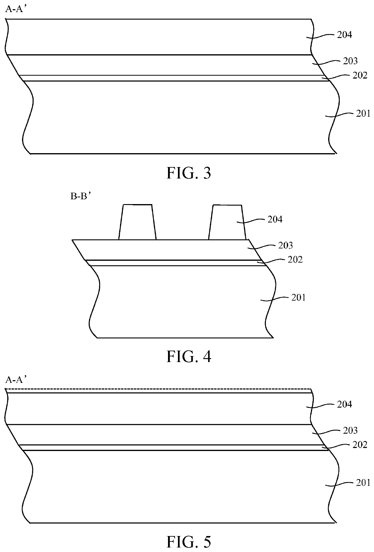
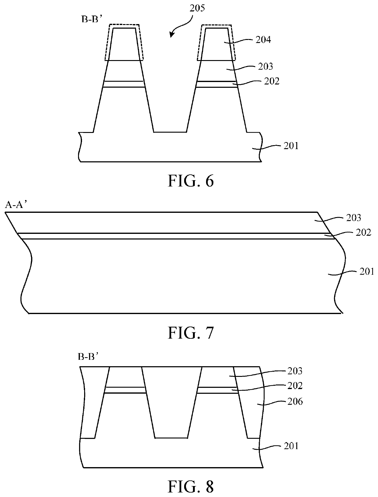
The present invention describes a non-volatile memory with a floating gate structure having two sharp portions and a corner. The corner is not covered by a control gate structure. The tunneling dielectric layer covers the sharp portions and the tip of the corner. During an erase operation, electrons are injected into the erasing gate structure from the sharp portions, improving erase efficiency. The sharp portions and corner increase the thickness of the tunneling dielectric layer, preventing leakage current and improving data retention. The manufacturing method is simple and practical.

Problems solved by technology

Non-volatile memory cell of a single-transistor stack gate structure always has problem in the case of excessive erase.
For example, when an excessive erase operation has already occurred in an unselected cell, the cell will generate a leakage current during a read operation.
This arouses another problem, that is, the complex circuit layout will lead to a large memory cell size, which does not meet a miniaturization requirement of products.
However, the memory cell with the double-transistor structure is obviously larger in size than the memory cell with the single-transistor structure, and the issue of the size of the memory cell is not solved yet.
However, the technical solution of the U.S. Pat. No. 7,868,375B2 still has a problem.
A thin tunneling dielectric layer easily causes current leakage, and electric charge stored in the floating gate will leak to the erasing gate and be erased, thereby causing poor data retention.

Method used


Image

  • Non-volatile memory and manufacturing method for the same
  • Non-volatile memory and manufacturing method for the same
  • Non-volatile memory and manufacturing method for the same

Examples


Embodiment Construction

[0076]Implementations of the present invention are illustrated below through specific embodiments. Persons skilled in the art can easily understand other advantages and efficacy of the present invention according to the content disclosed in this specification. The present invention can also be implemented or applied through other different specific implementations. Various modifications or variations can also be made on details in this specification based on different opinions and applications without departing from the spirit of the present invention.

[0077]Refer to FIGS. 1 to 43. It should be noted that, the figures provided in this embodiment merely illustrate the basic conception of the present invention schematically. Therefore, the figures only show components related to the present invention, and are not drawn according to the quantity, shapes and sizes of components during actual implementation. The pattern, quantity and ratio of components during actual implementation can be...


PUM

PropertyMeasurementUnit
heightaaaaaaaaaa
thicknessaaaaaaaaaa
thicknessaaaaaaaaaa

Abstract

The present invention provides a non-volatile memory and a manufacturing method for the same. In the non-volatile memory, a floating gate structure has a first sharp portion and a second sharp portion, and a corner formed by a side surface of the floating gate structure and a part of a top surface of the floating gate structure is not covered by a control gate structure. The corner is connected between the first sharp portion and one end of the second sharp portion. A tunneling dielectric layer of an erasing gate structure covers the first sharp portion, the second sharp portion, and a tip part of the corner.

Description

BACKGROUND OF THE PRESENT INVENTIONField of Invention[0001]The present invention belongs to the technical field of semiconductor, and in particular, to a non-volatile memory and a manufacturing method for the same.Description of Related Arts[0002]A non-volatile memory (NVM) refers to a computer memory in which the stored data will not disappear when power supply is turned off. Non-volatile memories can be classified into two major categories: read-only memories (ROMs) and flash memories, depending on whether data stored in a memory can be rewritten at any time while a computer is used. For the read-only memory: data cannot be changed or deleted once being stored, and content will not disappear after a power supply is turned off Therefore, the read-only memory is usually used for storing programs or data that does not need to be changed in an electronic system or a computer system. The flash memory is an electrically erasable programmable read-only memory which allows erase or write ...

Claims


Application Information

Patent Timeline
Patent Type & Authority Applications(United States)
IPC IPC(8): H01L29/788H01L29/78H01L29/66H01L21/762H01L21/3213H01L21/265H10B41/00H10B41/30
CPCH01L29/66825H01L21/265H01L21/32139H01L21/76224H01L29/788H01L29/7831H10B41/00H10B41/30H01L29/42344H01L29/40114H01L29/7885H01L21/283H01L29/42328H01L21/02107H01L21/02697
Inventor CHERN, GEENG-CHUAN
Owner NEXCHIP SEMICON CO LTD
Learn More