
Resistive memory

a memory array and resistance element technology, applied in the direction of digital storage, semiconductor/solid-state device details, digital storage, etc., can solve the problems of complex memory array manufacturing and attention-grabbing resistive memories using variable resistance elements, and achieve high reliability

Active Publication Date: 2020-04-09
WINBOND ELECTRONICS CORP
View PDF0 Cites 2 Cited by
  • Summary
  • Abstract
  • Description
  • Claims
  • Application Information

AI Technical Summary

Benefits of technology

The invention reduces the number of bit lines or source lines in the memory array, which reduces the size of the array and allows for larger line width. This reduces resistance and improves performance and reliability in writing and reading to memory cells.

Problems solved by technology

For non-volatile memories that replace flash memories, resistive memories using variable resistance elements are attracting attention.
Thus, the symmetry of the circuit is necessary, so that the manufacture of the memory array becomes more complicated than the unipolar type.

Method used


Image

  • Resistive memory
  • Resistive memory
  • Resistive memory

Examples


first embodiment

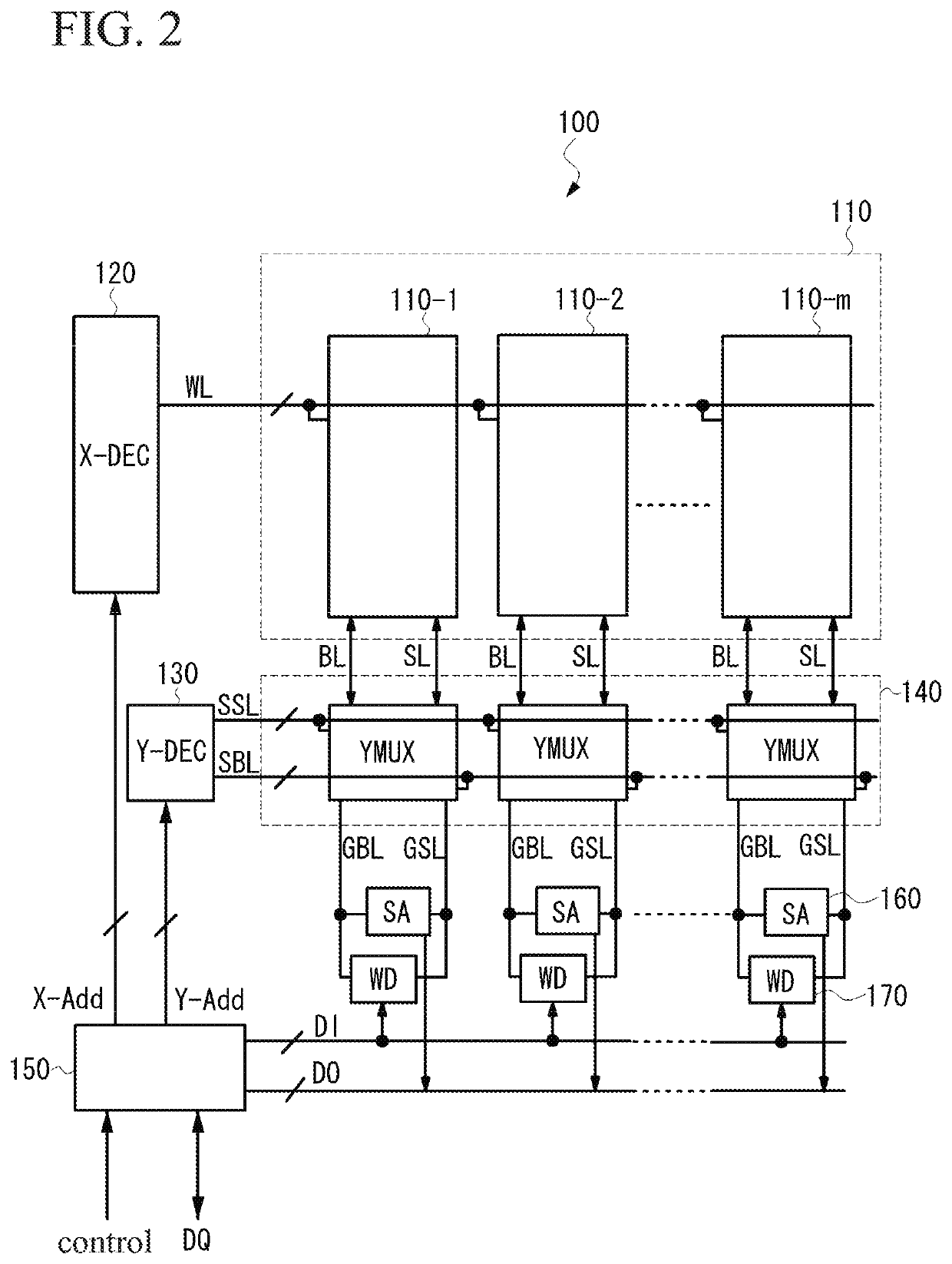
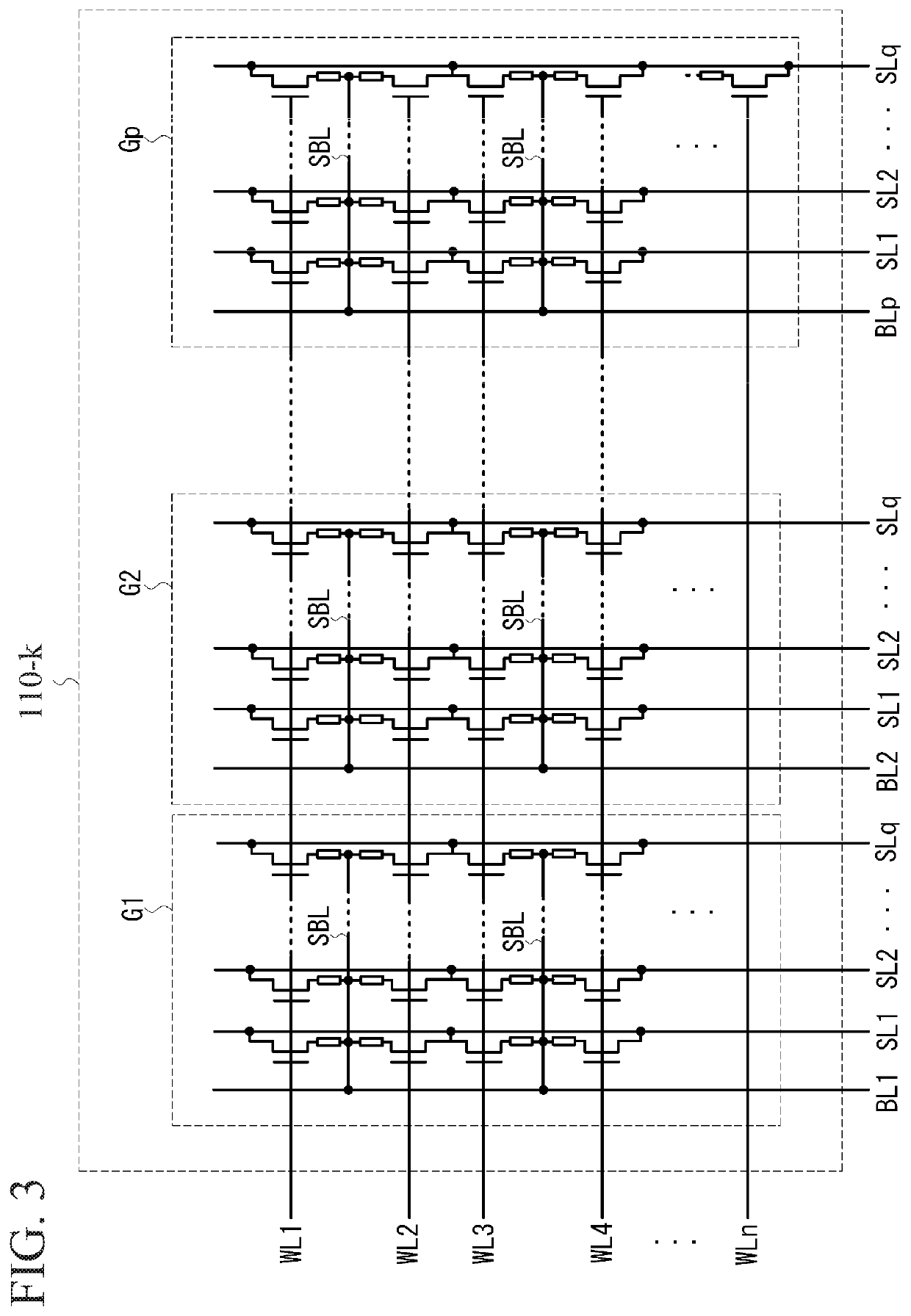
[0048]In the present invention, the memory array 110 has a configuration in which the bit lines are shared. In the following description, the bit lines and the source lines which extend from the column selection circuits 140 to the memory array 110 and are orthogonal to the word lines WL are referred to as the local bit lines BL and the local source lines SL, respectively. A bit line which extends from the local bit line BL and is in parallel with the word lines WL is referred to as a shared bit line SBL.

[0049]In FIG. 3, only the k-th sub-array 110-k of the memory array 110 is shown for example. It should be noted that the other sub-arrays have the same configuration.

[0050]The sub-array 110-k is divided into p groups G1, G2, . . . , Gp in the row direction, and one group comprises memory cells arranged on n rows and q columns. A memory cell comprises an accessing transistor and a variable resistance element coupled to the accessing transistor in series. The variable resistance eleme...

second embodiment

[0083]FIG. 17 is a cross-sectional view (line Y2-Y2) showing a modification of the In the above embodiment, since the local source line is separated from the memory cells which are disposed directly below the local source line, the via contacts V2 / C2 are not formed. In this case, if the via contacts are not formed in a partial area of the memory array, there is a possibility that the dimensional accuracy of the surrounding memory cells is adversely affected. Therefore, in the modification, as shown in FIG. 17, the local source line SL2 is connected to the memory cells, which are disposed below the local source line SL2, through the via contacts V2 / C2 whose size is the same as the memory cells. That is, there is a short circuit formed between the local source line SL2 and the transition metal oxide TMO through the via contacts V2, so that, the formation of the memory cells including the dummy cell can be made uniform. Since there is a short circuit formed between the corresponding b...


PUM


Abstract

The invention provides a resistive memory with better area efficiency without degrading reliability, which includes an array area, word lines, a local bit line, source lines, and a shared bit line. In the array area, memory cells are arranged in a matrix, and each memory cells includes a variable resistance element and an accessing transistor. The word lines extend in a row direction of the array area and are connected to the memory cells in the row direction. The local bit line extends in a column direction of the array area. The source lines extend in the column direction and are connected to first electrodes of the memory cells in the column direction. The shared bit line is connected to the local bit line. The shared bit line extends in the row direction and is connected to second electrodes of the memory cells in the row direction.

Description

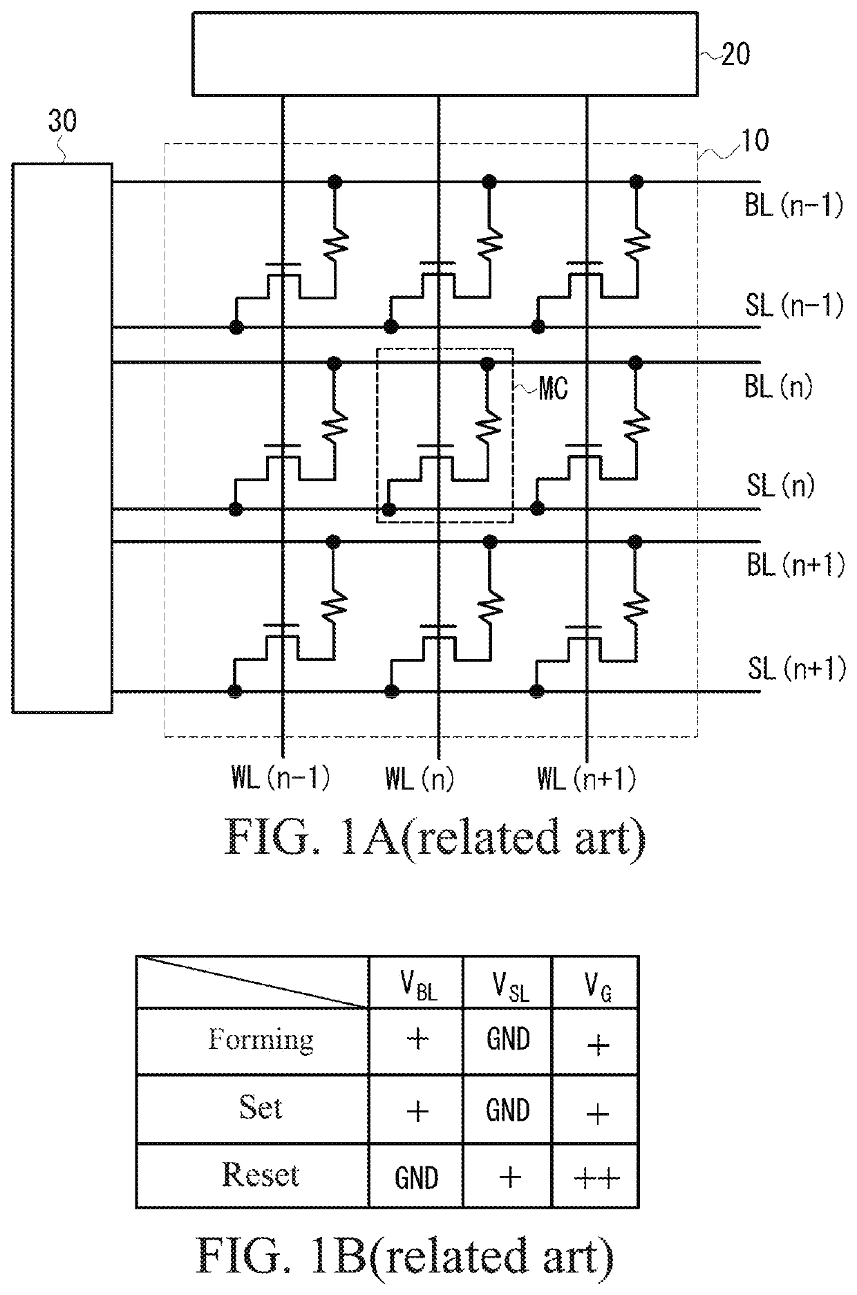
CROSS REFERENCE TO RELATED APPLICATIONS[0001]This application claims priority of Japan Patent Application No. 2018-188003, filed on Oct. 3, 2018, the entirety of which is incorporated by reference herein.BACKGROUND OF THE INVENTIONField of the Invention[0002]The invention relates to a resistive random-access memory using resistive elements, and more particularly to a structure of a memory array.Description of the Related Art[0003]For non-volatile memories that replace flash memories, resistive memories using variable resistance elements are attracting attention. It is known that resistive memories are memories whose variable resistance elements are applied by pulse voltages, such that the variable resistance elements reversibly and non-volatilely become a high resistive state or a low resistive state to memorize information. The resistive memories have the following advantages: since data can be overwritten with a low voltage (in a small amount of current), the power consumption is ...

Claims


Application Information

Patent Timeline
IPC IPC(8): H01L27/24H01L23/528H01L23/522H01L45/00G11C13/00
CPCH01L45/146G11C2213/32G11C2013/005H01L27/2436G11C13/0007G11C13/0069H01L45/1233G11C13/004H01L23/528H01L27/2463H01L23/5226G11C13/0097G11C2213/79G11C2013/009G11C13/0004G11C13/0026G11C13/0028H01L27/0207H10B63/30G11C13/0023G11C13/003G11C2013/0083G11C2213/82G11C13/0061H10B63/80H10N70/20H10N70/8833H10N70/231H10N70/826
Inventor TOMITA, YASUHIROLIN, CHI SHUN
Owner WINBOND ELECTRONICS CORP
Learn More