
Chip-scale linear light-emitting device

Active Publication Date: 2019-09-26
MAVEN OPTRONICS CO LTD
View PDF7 Cites 2 Cited by
  • Summary
  • Abstract
  • Description
  • Claims
  • Application Information

AI Technical Summary

Benefits of technology

This patent describes a chip-scale linear light-emitting device that can be used as a light source in a backlight module. The device emits light with a linearly and uniformly distributed light radiation pattern. By using a reflective structure, the device can effectively minimize or reduce dark regions on the light guide plate. The device also has a perpendicular main light-emitting surface, which makes it easy to align with the light guide plate to avoid light leakage. The device can be used as a side-view type chip-scale linear light-emitting device that can be accurately aligned with the light guide plate to avoid light leakage. Overall, the device provides a uniform light beam with a linearly distributed light radiation pattern, which can be more effectively utilized in the backlight module.

Problems solved by technology

In other words, the light beam intensity provided by the LED light bar is not continuously and is not uniformly distributed along the length direction of the light bar.
With this configuration, it is challenging to accurately align the miniaturized LED light bar module with the light-incident surface of the thin light guide plate, resulting in light leakage.

Method used


Image

  • Chip-scale linear light-emitting device
  • Chip-scale linear light-emitting device
  • Chip-scale linear light-emitting device

Examples


first embodiment

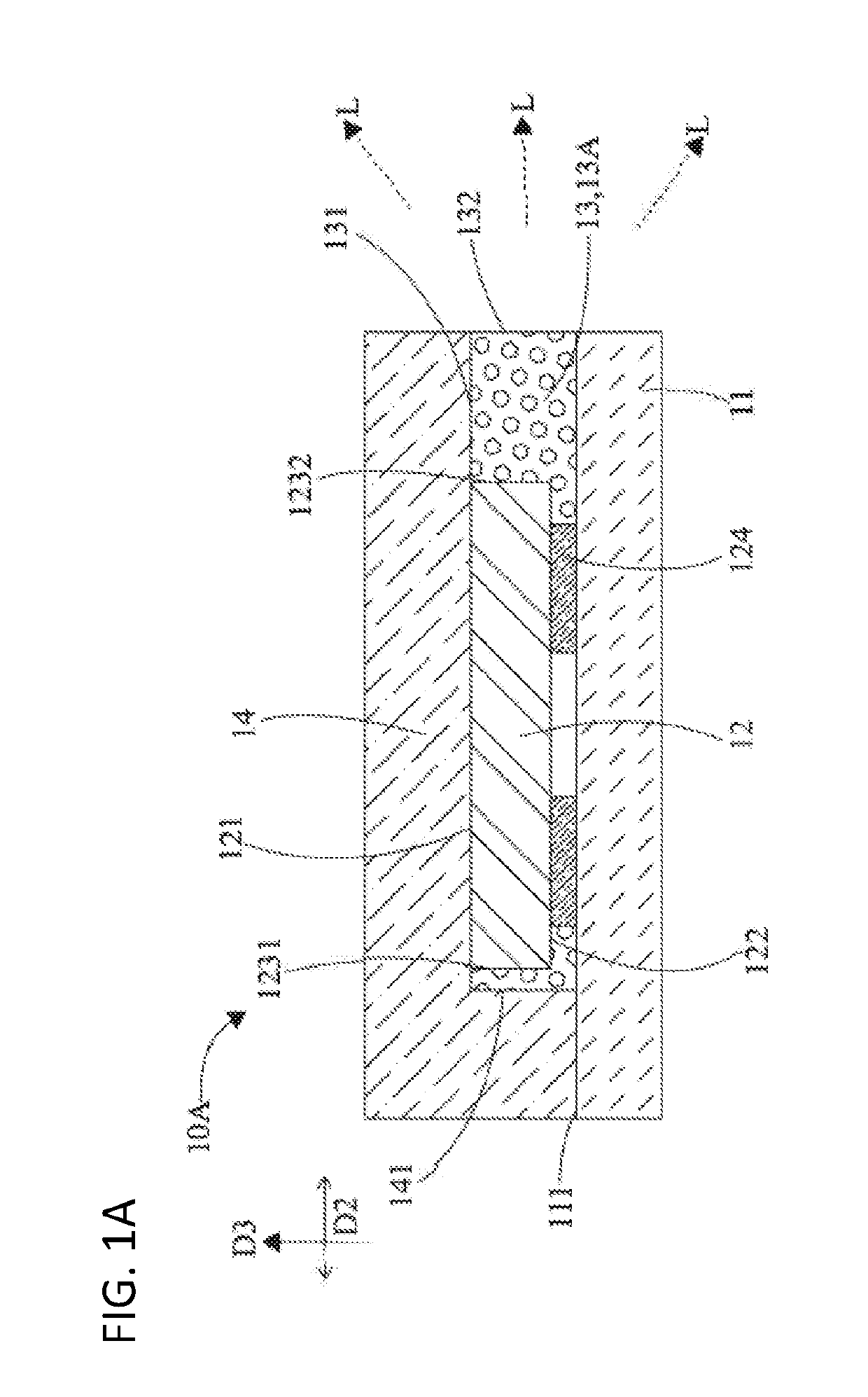
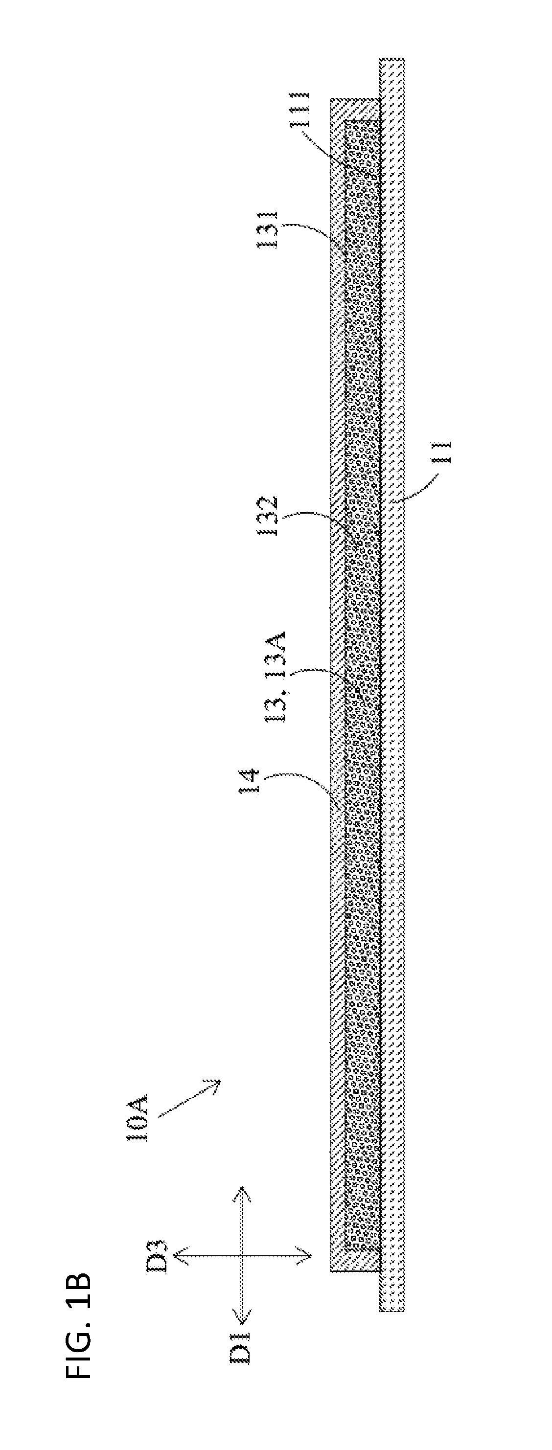
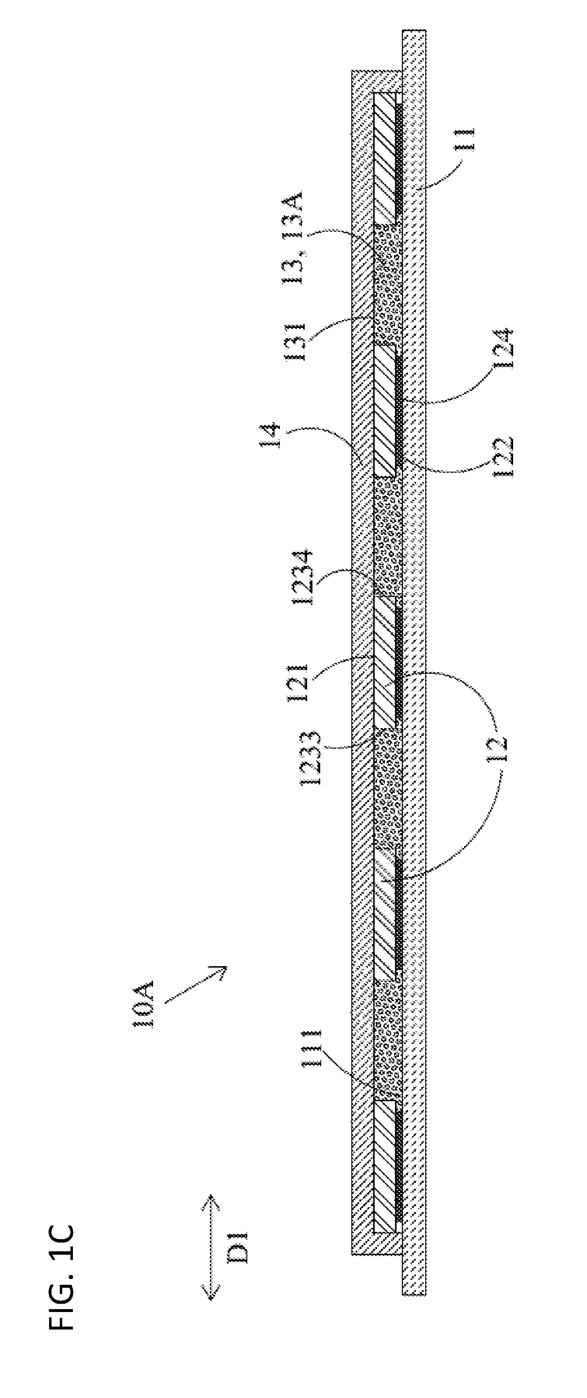
[0047]As illustrated from FIG. 1A to FIG. 1C are a side cross sectional view, a front view and a front cross-sectional view of a chip-scale linear light-emitting device 10A according to the present disclosure. The linear light-emitting device 10A can provide a linearly and uniformly distributed light radiation pattern so as to reduce dark areas formed on a light-incident surface 21 of a light guide plate 20 (as shown in FIG. 15A, FIG. 15B, FIG. 16A, and FIG. 16B). The linear light-emitting device 10A can include a linear and rectangular submount substrate 11, a plurality of LED semiconductor chips 12, a chip-scale packaging structure 13 (hereinafter referred to as the packaging structure 13), and a reflective structure 14. The technical details of each component are described in the following order.

[0048]The submount substrate 11 is provided so that other components of the linear light-emitting device 10A can be disposed thereon, and may be a good reflector to prevent the light beam...

second embodiment

[0071]As illustrated in FIG. 3A and FIG. 3B are a side view and a front cross-sectional view, respectively, of a chip-scale linear light-emitting device 10B according to the present disclosure. The linear light-emitting device 10B differs from the above-described linear light-emitting device 10A, which is specified to provide a linear light beam by mixing a primary light and a converted secondary light to generate a white light or the like, in that the packaging structure 13 is, or includes, a light-transmitting element 13B, which is specified to directly cover the second chip-edge surface 1232 of the LED semiconductor chip 12.

[0072]Specifically, the packaging structure 13 does not include color conversion materials such as the photoluminescent element 13A capable of converting the wavelength of the light beam, and includes the light-transmitting element 13B that does not substantially affect the wavelength of the primary light radiated from the LED semiconductor chips 12. The light...

third embodiment

[0075]As illustrated in FIG. 5A and FIG. 5B are a side cross-sectional view and a front cross-sectional view, respectively, of a chip-scale linear light-emitting device 10C according to the present disclosure. The linear light-emitting device 10C is also configured to provide white light or the like, and the linear light-emitting devices 10C and 10A are structurally different, at least in that the packaging structure 13 of the linear light-emitting device 10C includes a photoluminescent element 13A and a light-transmitting element 13B, wherein the light-transmitting element 13B directly covers the second chip-edge surface 1232 of the LED semiconductor chip 12, and the photoluminescent element 13A directly covers one light-transmitting-element-side surface 13B1 (e.g., an outer side surface) of the light-transmitting element 13B to indirectly cover the LED chip-edge surface 1232 of the LED semiconductor chip 12. The light-transmitting-element-side surface 13B1 and the chip-edge surfac...


PUM


Abstract

A chip-scale linear light-emitting device includes a submount substrate, light-emitting diode (LED) semiconductor chips, a chip-scale packaging structure and a reflective structure. The LED semiconductor chips, the packaging structure and the reflective structure are disposed on the submount substrate, wherein the packaging structure partially covers the chip-upper surface and / or the chip-edge surfaces of the LED semiconductor chips, and the reflective structure partially covers the package-top surface and / or the package-side surfaces of the packaging structure. If one of the chip-edge surfaces and the package-side surface of the packaging structure are exposed from the reflective structure as a primary light-emitting side surface, a side-view type linear light-emitting device is formed. If the package-top surface of the packaging structure is exposed from the reflective structure as a primary light-emitting top surface, a top-view type linear light-emitting device is formed. A substantially transparent light-transmitting material and / or a photoluminescent material can be configured to be included inside the packaging structure. In this configuration, a primary light emitted from the LED semiconductor chips is directed to pass through the packaging structure and radiated outward from the primary light-emitting surface. Therefore, a monochromatic light or a white light with a uniformly distributed linear radiation pattern can be generated using the chip-scale linear light-emitting device.

Description

CROSS-REFERENCE TO RELATED APPLICATIONS[0001]This application claims the benefit of and priority to Taiwan Patent Application No. 107110390 filed on Mar. 23, 2018, and Chinese Patent Application No. 201810254467.7 filed on Mar. 26, 2018, the disclosures of which are incorporated herein by reference in their entirety.BACKGROUNDTechnical Field[0002]The present disclosure relates to a light-emitting device, and more particularly to a chip-scale linear light-emitting device having a uniformly distributed linear radiation pattern.Description of the Related Art[0003]Light-emitting diodes (LEDs) have been used in an edge-lit type backlight module or a direct backlight module of a Liquid Crystal Display (LCD) for televisions and smart phones. An edge-lit backlight module generally includes a light guide plate and an LED light bar, wherein the LED light bar is disposed beside one side surface of the light guide plate (hereinafter referred to as a light-incident surface). The LED light bar ca...

Claims


Application Information

Patent Timeline
IPC IPC(8): H01L27/15H01L33/60H01L33/50F21V8/00
CPCH01L27/156H01L33/60G02B6/0073H01L33/56H01L33/507H01L2933/0033H01L33/486H01L2933/0058G02B6/0026G02B6/0031
Inventor CHEN, CHIEHCHANG, CHIA-HSIEN
Owner MAVEN OPTRONICS CO LTD
Learn More