
Method of manufacturing thermoelectric module using ink formulations

a thermoelectric module and ink formulation technology, applied in the direction of sustainable manufacturing/processing, non-metal conductor manufacturing, final product manufacturing, etc., can solve the problems of poor drying properties of solvents which may otherwise represent suitable candidates for printing ink compositions, difficult solvent selection of doped conductive polymers, and high toxicities, etc., to achieve excellent electrical conductivity and improve performan

Inactive Publication Date: 2019-08-01
CAMBRIDGE DISPLAY TECH LTD +1
View PDF0 Cites 2 Cited by
  • Summary
  • Abstract
  • Description
  • Claims
  • Application Information

AI Technical Summary

Benefits of technology

This patent describes a way to create a stable mixture of polymer and dopant that can be used to create highly conductive layers. By using high solids content and multi-pass printing, thick layers of thermoelectric material can be deposited which lead to improved performance of thermoelectric modules.

Problems solved by technology

However, in thermoelectric organic materials there is a well-known trade-off between electrical conductivity and Seebeck coefficient, which severely limits the development of organic thermoelectric generators.
While it is widely known that the choice of processing solvents may generally have a significant influence on the morphology of the solution-deposited conductive layer, the deposition of doped conductive polymers is particularly challenging from the viewpoint of solvent selection.
For example, a number of solvents which may otherwise represent suitable candidates for printing ink compositions tend to exhibit poor drying properties and / or a high toxicity, such as halogenated solvents (e.g. chlorobenzene, dichlorobenzenes).
However, a large number of applications require extended printing times. For instance, in order to provide thermoelectric legs with a sufficient layer thickness, multiple printing passes are required, which may extend the printing process to the range of hours, during which increased precipitation may occur.
On the other hand, the conventional approach of avoiding precipitation by reducing the solids content in the ink composition is not suitable for the printing of thick layers.
Accordingly, ink compositions prone to precipitation cannot be used with satisfactory results.

Method used


Image

  • Method of manufacturing thermoelectric module using ink formulations
  • Method of manufacturing thermoelectric module using ink formulations
  • Method of manufacturing thermoelectric module using ink formulations

Examples


example 1

[0068]A dispersion has been prepared by separately dissolving PQT12 in 1,2,4-trimethylbenzene (TMB; δD=18.0; δP=1.0; δH=1.0) as the first solvent at a concentration of 1.29% w / v, and the dopant F4TCNQ in acetonitrile (δP=18.0) as the second solvent at a concentration of 0.33% w / v. The dissolution of PQT12 has been accelerated by heating to 80° C. The solutions were then combined with mixing and subjected to sonication at 37 kHz for 1 hour, resulting in a stable dispersion having a polymer:dopant ratio of 9:1 by weight and TMB:acetonitrile ratio of 7:3 by volume, the dispersion comprising doped polymer particles suspended within the solvent blend and having a solids content of 1%.

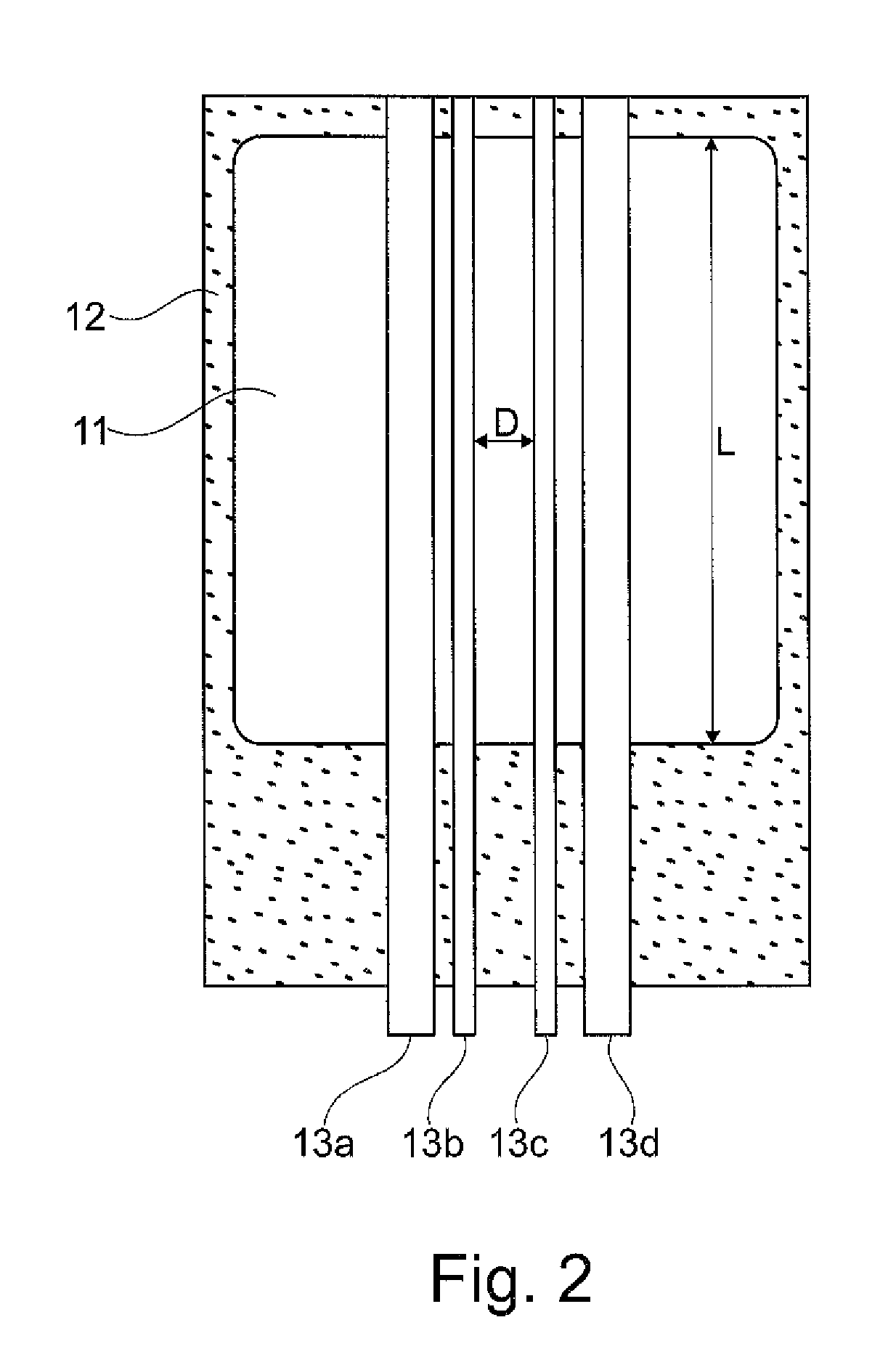
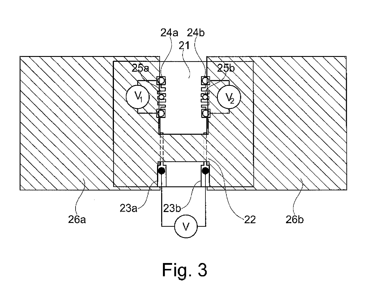
[0069]Thereafter, devices having a configuration in accordance with FIG. 2 have been manufactured. For this purpose, substrates have been prepared by evaporating or sputtering onto glass a layer of chrome / gold or AgBiGe, respectively. These were patterned by photolithography to form 4 point probe electrode c...

example 2

[0075]In a further example, a dispersion has been prepared in accordance with Example 1, with the exception that anisole (δD=17.8; δP=4.1; δH=6.7) has been used as the first solvent for PQT12 and acetone (δP=10.4) as the second solvent for F4TCNQ. The conductivity a of the conductive film measured in a device prepared in analogy to Example 1 was determined to be 0.1 S / cm.

[0076]Accordingly, it has been shown that the formulation according to the present invention has sufficient stability for solution deposition methods and enables manufacture of conductive layers having both excellent conductivity and thermopower.

[0077]Once given the above disclosure, many other features, modifications, and improvements will become apparent to the skilled artisan.

[0078]In some examples, the first solvent may take the form of a blend of electron-rich organic compounds, each comprising one or more electron-donating groups. In other words, the first solvent may be a blend of two or more solvents, each h...


PUM

PropertyMeasurementUnit
Electrical conductivityaaaaaaaaaa
Boiling pointaaaaaaaaaa
Energyaaaaaaaaaa

Abstract

A method of manufacturing a conductive layer includes the step of dissolving an organic semiconductor polymer in a first solvent, the first solvent being an aromatic or heterocyclic compound comprising one or more electron-rich carbon atom(s) and / or heteroatom(s). The method also includes dissolving a dopant in a second solvent, the second solvent being a polar solvent. The method also includes mixing the solutions of the organic semiconductor polymer and the dopant to form a dispersion comprising doped conductive polymer particles suspended in the solvent blend. The method also includes depositing the dispersion by a solution deposition technique to form a conductive layer. The solution deposition technique is preferably an inkjet printing, dispense printing or drop casting method. The dispersion provides a stable ink composition for the manufacturing of thick and uniform layers with excellent conductivity and thermopower, and allows simple fabrication of thermoelectric legs with enhanced performance.

Description

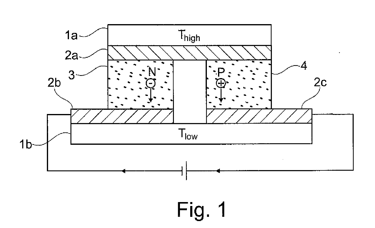
FIELD OF INVENTION[0001]This invention relates to a formulation comprising a dispersion of a doped conductive polymer in a blend of at least two solvents which is particularly useful as a stable ink formulation for solution deposition of highly conductive layers, e.g. in thermoelectric modules. In addition the present invention relates to a method of manufacturing conductive layers, conductive layers produced by said method and to thermoelectric modules comprising said conductive layers, e.g. as thermoelectric legs.BACKGROUND OF THE INVENTION[0002]Organic thermoelectrics have attracted considerable research interest since they enable realization of flexible, large-area modules which may be manufactured and processed at low costs by using solution processing techniques.[0003]In general, the fabrication of a thermoelectric module involves the formation of p- and n-type semiconducting legs that are usually connected in series to the applied electric field and parallel to the heat gradi...

Claims


Application Information

Patent Timeline
IPC IPC(8): H01L35/24H01B1/12C08G61/12
CPCH01L35/24H01B1/127C08G61/126C08G2261/792C08K5/315C08K5/56Y02E10/549Y02P70/50H10N10/856H10N10/01H10K71/15H10K71/611H10K85/113C08L65/00C09D5/24C09D165/00H01B1/12
Inventor FLETCHER, THOMAS
Owner CAMBRIDGE DISPLAY TECH LTD
Learn More