
Broadband mirror

a mirror and wideband technology, applied in the field of broadband mirrors, can solve the problems of inability to achieve 100% reflectivity, dbr may only effectively reflect light within a limited range of wavelengths and angles of incidence, etc., to achieve the effect of improving the reflectance of the planar layer stack, increasing reflection, and reducing transmission

Active Publication Date: 2019-05-02
LUMILEDS
View PDF8 Cites 0 Cited by
  • Summary
  • Abstract
  • Description
  • Claims
  • Application Information

AI Technical Summary

Benefits of technology

The invention is a broadband mirror that improves reflectivity by incorporating roughened dielectric layers in the layer stack. This results in a significant improvement in reflectivity over a wide range of angles of incidence and wavelengths. The patterned interface between the layers causes scattering in the light-emitting layer, which is beneficial for light outcoupling from the device. The method for creating the broadband mirror requires minimal effort and can be done using existing techniques. The invention is based on the idea that a patterned interface between dielectric layers with different refractive indices can significantly increase the reflectance of the planar layer stack. The reflectivity of the broadband mirror can be further improved by increasing the number of patterned layer interfaces.

Problems solved by technology

However, a disadvantage of a DBR is its wavelength-dependency, since a specific DBR can only reflect light within certain band of wavelengths.
Therefore, a DBR may only effectively reflect light within a limited range of wavelengths and angles of incidence.
However, it is impossible to achieve 100% reflectivity, and a metal reflective backing layer will therefore absorb some percentage of the light that reaches it instead of returning it to the emission face of the die.
A further disadvantage of the reflective metal layer is its temperature dependence, since care must be taken to ensure reliable operation of the device within a safe temperature range.
However, high temperatures arising at a p-n diode junction in such a composite die may cause problems for a metal reflective backing.
A metal that is a good optical reflector for an LED may however cause reliability problems when the LED operates at high temperatures.
Even so, the net reflectance of such a composite die may not be sufficient for some applications.

Method used


Image

  • Broadband mirror
  • Broadband mirror
  • Broadband mirror

Examples


first embodiment

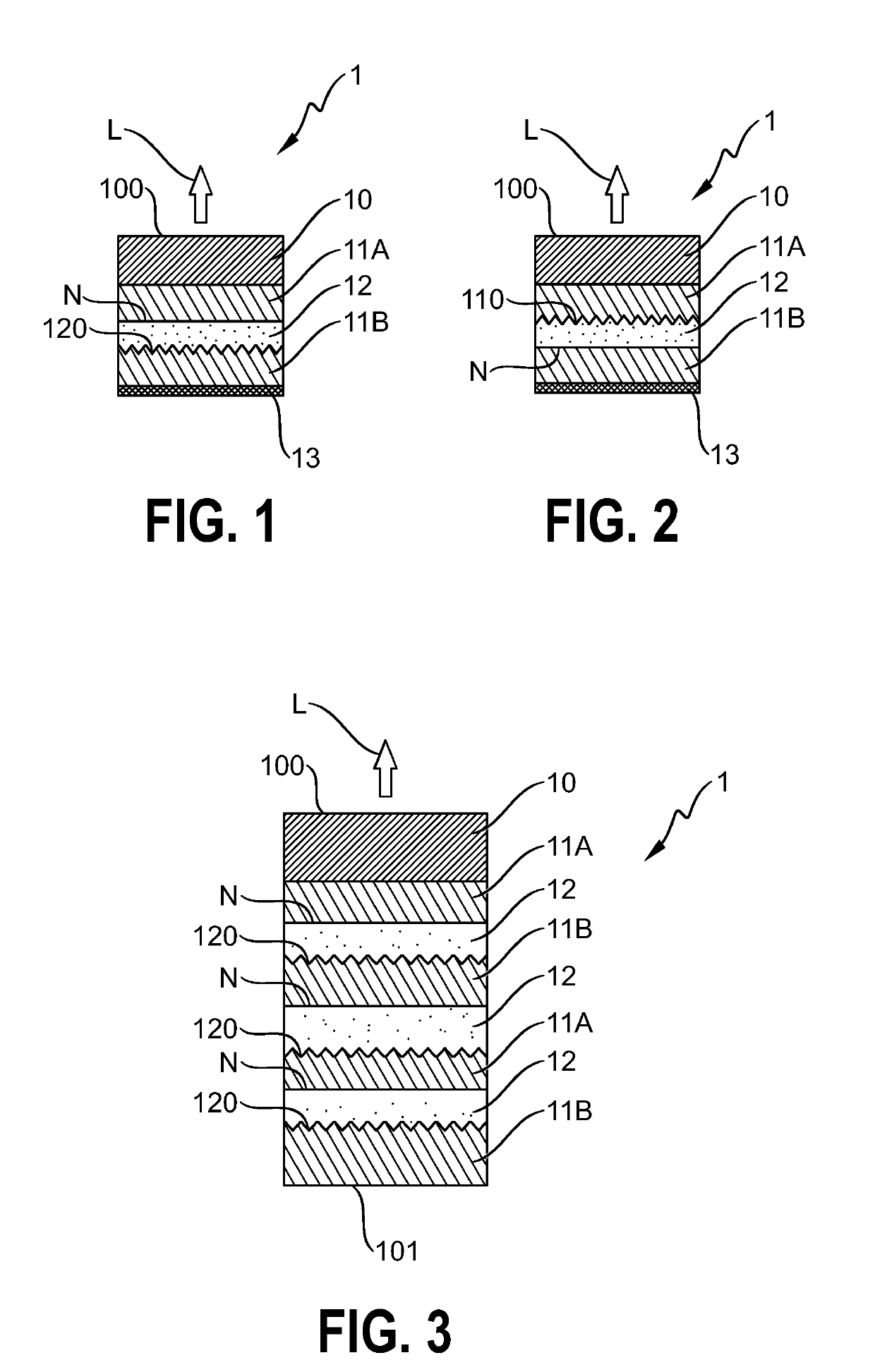
[0032]FIG. 1 shows the broadband mirror 1 according to the invention (in this and the following diagrams, composite die multilayer stacks are shown with exaggerated proportions; the height of a composite die is generally in the range of 5 μm to 15 μm). In this exemplary embodiment, the broadband mirror 1 is constructed as a composite die comprising a stack of four planar layers 10, 11A, 12, 11B and a reflective backing 13. Layers 11A, 12, 11B of suitable material are deposited one after each other, and the final layer 11B is terminated by a reflective backing 13. The planar layers 11A, 12, 11B can be built up in the usual manner, by vapour deposition or any other suitable technique, starting with an uppermost layer 10 and working “downwards”, applying a first low-index layer 11A, a high index layer 12, and a second low-index layer 11B Using the inventive method, the high-index layer 12 is applied to the non-patterned surface N of the first adjacent low-index layer 11A. The surface o...

second embodiment

[0034]FIG. 2 shows the broadband mirror 1 according to the invention. Here also, the broadband mirror 1 is constructed as a stack of four planar layers 10, 11A, 12, 11B and a reflective backing 13. In this embodiment, the surface of the first low-index layer 11A is patterned or roughened before depositing the high-index layer 12. A second low-index layer 11B is applied to the non-patterned surface N of the high-index layer 12. The patterned surface 110 of the first high-index layer 12A, in conjunction with the low-index / high-index boundary, also acts to prevent photons from passing in the direction of the reflective backing 13, and effectively re-directs them towards the light emission face 100 as described above.

third embodiment

[0035]FIG. 3 shows the broadband mirror 1 according to the invention. In this embodiment, the broadband mirror 1 is constructed as a stack of eight planar layers 10, 11A, 12, 11B. Three high-index layers 12 are sandwiched between low-index layers 11A, 11B. Each high-index layer 12 is applied to the non-patterned surface N of the preceding low-index layer 11A, 11B. The surface of each high-index layer 12 is roughened before depositing the subsequent low-index layer 11A, 11B. Since each high-index layer 12 (with its roughened surface 120) effectively “sends back” more photons in the direction of the light emission face 100 than it “lets through”in the opposite direction, the net result of using several such high-index layers 12 is that little or no photons make it to the lowermost face 101 of the mirror 1. Therefore, there is no need to apply a reflective backing to this rear face 101. There are advantages associated with not requiring a reflective backing, namely a saving in cost as ...


PUM


Abstract

The invention describes a broadband mirror comprising an outer surface layer; and a dielectric layer stack arranged underneath the outer surface layer; characterized in that the dielectric layer stack comprises at least one patterned surface at an interface between adjacent dielectric layers of the dielectric layer stack. The invention further describes a light-emitting diode. The invention also describes a method of manufacturing a broadband mirror, which method comprises the steps of providing an outer surface layer and applying a plurality of dielectric layers to build a dielectric layer stack underneath the outer surface layer, characterized by the step of patterning the surface of at least one dielectric layer before applying a subsequent dielectric layer to the patterned surface.

Description

FIELD OF THE INVENTION[0001]The invention describes a broadband mirror, a light-emitting diode, and a method of manufacturing a broadband mirror.BACKGROUND OF THE INVENTION[0002]Broadband mirrors are used to maximize the efficiency of optical systems and maintain colour integrity. For example, increasing the reflectivity of mirrors used in light engines and projectors is directly related to an improvement or increase in brightness. A distributed Bragg reflector (DBR) is one kind of semiconductor mirror, comprising many layers of precisely deposited material. However, a disadvantage of a DBR is its wavelength-dependency, since a specific DBR can only reflect light within certain band of wavelengths. Light outside this band will not be reflected by the multilayer stack. Furthermore, the reflectivity response of a DBR may depend on the angle of incidence of the light. Therefore, a DBR may only effectively reflect light within a limited range of wavelengths and angles of incidence.[0003...

Claims


Application Information

Patent Timeline
Patent Type & Authority Applications(United States)
IPC IPC(8): H01L33/46G02B5/08
CPCH01L33/46G02B5/0808H01L2933/0025G02B5/28H01L33/58
Inventor LOPEZ, TONIJIN, FAHONG
Owner LUMILEDS
Learn More