
Retrieval apparatus and retrieval method

a technology of retrieval apparatus and retrieval method, which is applied in the direction of adaptive control, semiconductor/solid-state device testing/measurement, instruments, etc., can solve problems such as inability, and achieve the effect of efficient operation and optimization of a process

Active Publication Date: 2019-02-28
HITACHI LTD
View PDF5 Cites 6 Cited by
  • Summary
  • Abstract
  • Description
  • Claims
  • Application Information

AI Technical Summary

Benefits of technology

The invention provides a way to efficiently operate and optimize a process in a semiconductor treatment apparatus. This can lead to improved performance and productivity.

Problems solved by technology

In a case where the time required for one retrieval is about one minute, one hundred thousand or more year is required for retrieval of all of the retrieval conditions, and this is not possible.

Method used


Image

  • Retrieval apparatus and retrieval method
  • Retrieval apparatus and retrieval method
  • Retrieval apparatus and retrieval method

Examples


example 1

[0043]Input Parameter Retrieval Examples

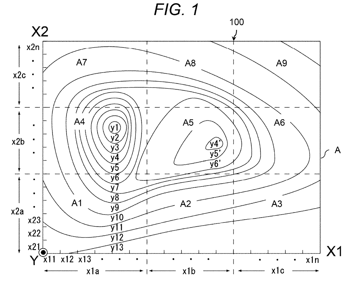
[0044]FIG. 1 is an explanatory diagram illustrating input parameter retrieval examples. FIG. 1 illustrates examples of combinations of input and output data, that is, input data and output data for a semiconductor treatment apparatus when input data (the above-described value of an input parameter) causing output data (the above-described value of an output parameter) satisfying a target to be obtained is retrieved in the semiconductor treatment apparatus.

[0045]Here, the semiconductor treatment apparatus is an apparatus treating a semiconductor or a semiconductor device including a semiconductor. Specifically, the semiconductor treatment apparatus includes, for example, a lithography apparatus, a film forming apparatus, a pattern processing apparatus, an ion implanting apparatus, a heating apparatus, and a cleaning apparatus. The lithography apparatus includes an exposure apparatus, an electron beam drawing apparatus, and an X-ray drawing appa...

example 2

[0168]In Example 2, in addition to region division in the above Example 1, a demonstration test is performed on the basis of a prediction model, and an optimal solution satisfying a target is retrieved. Thus, in Example 2, a prediction model is repeatedly updated by applying a result of a demonstration test (processing result) to learning data until a target is satisfied, and the target is gradually updated toward a final target such that an optimal solution is retrieved. A semiconductor manufacturing system has the same configuration as that in the above Example 1, and only a difference from the above Example 1 will be described with respect to the process content.

[0169]Input Parameter Retrieval Examples

[0170]FIG. 11 is an explanatory diagram illustrating input parameter retrieval examples. FIG. 11 illustrates examples of combinations of input and output data, that is, input data and output data for a semiconductor treatment apparatus when input data (the above-described value of a...


PUM


Abstract

A retrieval apparatus includes a processor and a memory and retrieves a condition given to a semiconductor treatment apparatus. The processor receives a processing result of a semiconductor, a condition corresponding to the processing result, a target value for treating the semiconductor, and a retrieval region. A prediction model is generated indicating a relationship between the condition and the processing result based on a set value of the condition in the retrieval region, and the processing result; calculates a predicted value, performs a demonstration test, acquires an actually measured value, outputs the predicted value as a set value when the actually measured value reaches the target value. When the actually measured value does not reach the target value, the prediction model is updated by applying the predicted value and the actually measured value to the set value and the processing result, respectively.

Description

CLAIM OF PRIORITY[0001]The present application claims priority from Japanese patent application JP 2017-161467 filed on Aug. 24, 2017, the content of which is hereby incorporated by reference into this application.BACKGROUND OF THE INVENTIONField of the Invention[0002]The present invention relates to a retrieval apparatus and a retrieval method for retrieving a solution.Background Art[0003]In order to improve performance of a semiconductor device, a new material forming the semiconductor device is introduced, and a structure of the semiconductor device is also complicated. The accuracy in a nanometer level is required in processing of a semiconductor device. In order to improve productivity of a semiconductor device, a mass-production process is required to be continuously performed as long as possible in a state of maintaining the accuracy. In order for a semiconductor device to satisfy the requirements, various kinds of materials and structures are required to be processed with co...

Claims


Application Information

Patent Timeline
Patent Type & Authority Applications(United States)
IPC IPC(8): G05B13/02H01L21/66G06N5/04
CPCG05B13/026H01L22/20G05B13/0265G06N5/046H01L22/12G06N20/00G06F30/20
Inventor OHMORI, TAKESHINAKADA, HYAKKAISHIKAWA, MASAYOSHIKURIHARA, MASARU
Owner HITACHI LTD
Learn More