Two-dimensional semiconductor saturable absorber mirror and fabrication method, and pulse fiber laser

a semiconductor saturable absorber and mirror technology, applied in the field of lasers, can solve the problem that commercial sesam is not suitable for the study of the dynamic characteristics of ultrafast fiber lasers, and achieve the effect of narrow operation bandwidth and low reliability of existing commercial sesam

Inactive Publication Date: 2018-12-27
SHENZHEN UNIV
View PDF5 Cites 6 Cited by
  • Summary
  • Abstract
  • Description
  • Claims
  • Application Information

AI Technical Summary

Benefits of technology

The present invention provides a two-dimensional semiconductor absorber mirror that overcomes the disadvantages of expensive and complex commercial SESAM, such as low reliability and narrow operational bandwidth. The two-dimensional semiconductor saturable absorber mirror includes an end surface of optical fiber, a two-dimensional semiconductor thin film, and a gold film, and has a high damage threshold, can be easily prepared in batch, and has high reliability. Additionally, it can be directly fused to the fiber laser system, making it easy to use and high in reliability. The pulse fiber laser made of the two-dimensional semiconductor saturable absorber mirror has the advantages of full utilization of fiber, high reliability, and ease of use and transformation.

Problems solved by technology

However, commercial SESAM is not suitable for the study on dynamic characteristics of ultrafast fiber laser due to its high price, complex fabrication process, narrow absorption bandwidth, output of only picosecond pulse and low damage threshold.

Method used


Image

  • Two-dimensional semiconductor saturable absorber mirror and fabrication method, and pulse fiber laser
  • Two-dimensional semiconductor saturable absorber mirror and fabrication method, and pulse fiber laser
  • Two-dimensional semiconductor saturable absorber mirror and fabrication method, and pulse fiber laser

Examples


Embodiment Construction

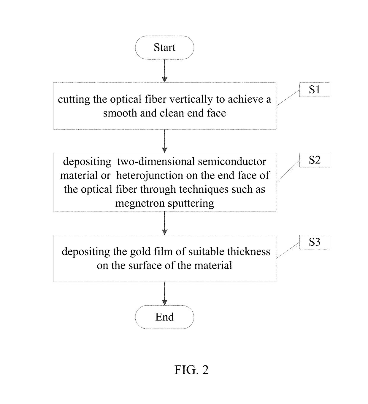
[0013]In order to make the objects, the technical solutions and the advantages of the present invention more clear and be better understood, the disclosure will be described in detail with reference to the accompanying drawings and embodiments.

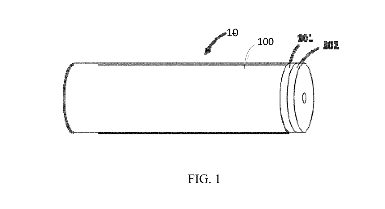
[0014]Referring to FIG. 1, a two-dimensional semiconductor saturable absorber mirror 10 is provided in the present disclosure. The two-dimensional semiconductor saturable absorber mirror 10 comprises an optical fiber 100, a two-dimensional semiconductor thin film 101 attached to an end surface of the optical fiber, and a high-reflecting film 102 attached to the two-dimensional semiconductor thin film 101. The optical fiber can be a single-mode fiber, a polarization-maintaining fiber, a high-gain active optical fiber (erbium-doped fiber, ytterbium-doped fiber, thulium-doped fiber, holmium-doped fiber, praseodymium-doped fiber, bismuth-doped fiber), or an active ZBLAN fiber.

[0015]The two-dimensional semiconductor thin film 101 can be made of any...


PUM


Abstract

A two-dimensional semiconductor saturable absorber mirror comprises an optical fiber, a two-dimensional semiconductor thin film attached to an end surface of the optical fiber, and a gold film attached to the two-dimensional semiconductor thin film. A method for fabricating the two-dimensional semiconductor saturable absorber mirror comprises the following steps: cutting the optical fiber, putting the cut optical fiber and a two-dimensional semiconductor target into a vacuum chamber, ionizing a surface of two-dimensional semiconductor target to generate two-dimensional semiconductor plasma, depositing the two-dimensional semiconductor plasma on an exposed end surface of the optical fiber to form the two-dimensional semiconductor thin film, and by controlling deposition time and / or deposition temperature, ensuring the two-dimensional semiconductor thin film to be a desired thickness; and plating the gold film on the resulting two-dimensional semi-conductor thin film.

Description

CROSS-REFERENCE TO RELATED APPLICATIONS[0001]This application is a continuation of International Patent Application No. PCT / CN2016 / 085986 with a filing date of Jun. 16, 2016, designating the United States, now pending. The content of the aforementioned applications, including any intervening amendments thereto, are incorporated herein by reference.TECHNICAL FIELD[0002]The present invention relates to the technical field of lasers, and more particularly to a two-dimensional semiconductor saturable absorber mirror and a fabrication method therefor, and a pulse fiber laser.BACKGROUND OF THE PRESENT INVENTION[0003]Passive mode locking is an effective way for fiber laser to realize ultrafast pulse output, and the key technique of passive mode-locking is the saturable absorption effect required in the resonator of the fiber laser. Researchers in the art have obtained passive mode-locking ultrafast pulse output in fiber lasers by using a variety of saturable absorption effects. Generally s...

Claims


Application Information

Patent Timeline
IPC IPC(8): H01S3/11H01S3/067H01S3/094
CPCH01S3/1118H01S3/0675H01S3/094003G02F1/3523H01S3/06712H01S3/08045H01S3/173
Inventor YAN, PEIGUANGCHEN, HAOXING, FENGFEIDING, JINFEI
Owner SHENZHEN UNIV
Why Eureka
Try Eureka