Antenna device
a technology of antenna array and antenna, applied in the field of antenna devices, can solve the problems of difficult application of ebg to a wideband antenna, complex substrate structure, and error in detection of targets, so as to improve the gain in the compensation direction, broaden the bandwidth, and simplify the configuration
- Summary
- Abstract
- Description
- Claims
- Application Information
AI Technical Summary
Benefits of technology
Problems solved by technology
Method used
Image
Examples
first embodiment
1. First Embodiment
[0041][1-1. Configuration]
[0042]An antenna device 1 is mounted inside a bumper of a vehicle and constitutes a millimeter-wave radar that detects various targets existing around the vehicle.
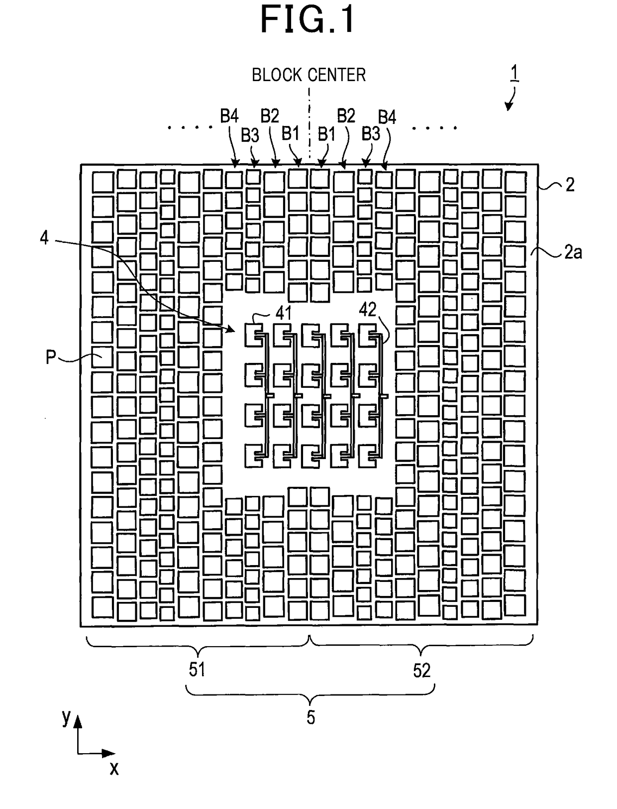
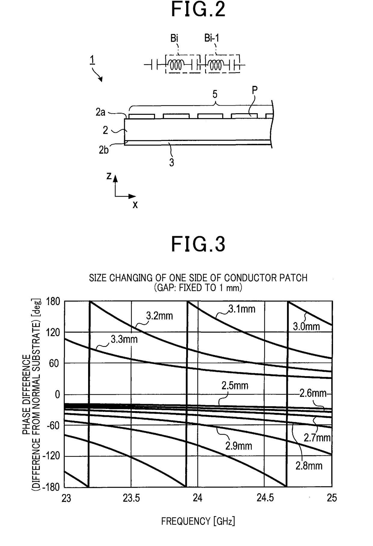
[0043]As shown in FIG. 1 and FIG. 2, the antenna device 1 is formed with copper patterns formed on a dielectric substrate 2 having a rectangular shape. In the following, the dielectric substrate 2 has one surface referred to as a substrate front surface 2a, and another surface referred to as a substrate back surface 2b. Additionally, a direction along one side of the dielectric substrate 2 is referred to as an x-axis direction, a direction along the other side orthogonal to the x-axis direction is referred to as a y-axis direction, and a normal direction of the substrate front surface 2a is referred to as a z-axis direction.
[0044]The substrate back surface 2b is formed with a ground plate 3 including a copper pattern covering the entire surface of the substrate back surface 2b. ...
second embodiment
2. Second Embodiment
[0069][2-1. Configuration]
[0070]An antenna device 6 is, for example, mounted in a vehicle, and used for a millimeter-wave radar for detecting various targets existing around the vehicle.
[0071]As shown in FIGS. 13 and 14, the antenna device 6 includes, a dielectric substrate 7 having a rectangular shape and a copper pattern formed on the dielectric substrate 7. In the following, the dielectric substrate 7 has one surface referred to as a substrate front surface 7a, and another surface referred to as a substrate back surface 7b. Additionally, a direction along a long side of the dielectric substrate 7 is referred to as an x-axis direction, a direction along the other short side orthogonal to the x-axis direction is referred to as a y-axis direction, and a normal direction of the substrate front surface 7a is referred to as a z-axis direction.
[0072]The substrate back surface 7b is formed with a ground plate 8 including a copper pattern covering the entire surface of...
PUM
 Abstract
Description
Claims
Application Information
 - R&D
- Intellectual Property
- Life Sciences
- Materials
- Tech Scout
- Unparalleled Data Quality
- Higher Quality Content
- 60% Fewer Hallucinations
Browse by: Latest US Patents, China's latest patents, Technical Efficacy Thesaurus, Application Domain, Technology Topic, Popular Technical Reports.
© 2025 PatSnap. All rights reserved.Legal|Privacy policy|Modern Slavery Act Transparency Statement|Sitemap|About US| Contact US: help@patsnap.com


