Semiconductor laser device, diffraction grating structure, and diffraction grating

a laser device and semiconductor technology, applied in the direction of laser optical resonator construction, laser details, laser output parameters control, etc., can solve the problems of easy variation of wavelength-tunable laser characteristics for each wavelength channel, increased frequency linewidth, and complex inspection process at the time of manufacture, etc., to achieve the effect of higher reflectivity

Active Publication Date: 2018-12-06
FURUKAWA ELECTRIC CO LTD
View PDF3 Cites 3 Cited by
  • Summary
  • Abstract
  • Description
  • Claims
  • Application Information

AI Technical Summary

Benefits of technology

[0018]According to a third aspect of the present disclosure, there is provided a vernier-type wavelength-tunable semiconductor laser device comprising an optical resonator, constituted by first and second reflective elements having reflection comb spectra in which reflection peaks are arranged on a wavelength axis in a substantially periodic manner and having mutually different periods, wherein at least one of the first and second reflective elements is a diffraction grating of a sampled grating structure including a plurality of diffraction grating structures, a plurality of sets of a high-refractive-index portion and a low-refractive-index portion having a lower refractive index than the high-refractive-index portion are alternately arranged in a predetermined direction in the diffraction grating structure, when a structure in which a plurality of sets of the high-refractive-index portion and the low-refractive-index portion are arranged in an alternately periodic manner is set as a basic structure, the diffraction grating structure has a structure formed by omitting at least one of the high-refractive-index portions from the basic structure, omitting at least one of the low-refractive-index portions, omitting at least one boundary between the high-refractive-index portion and the low-refractive-index portion, or performing a combination thereof, and the diffraction grating structure has a structure including a plurality of portions with alternating arrangement of the high-refractive-index portion and the low-refractive-index portion phase shifted by a ½ period from the basic structure.
[0019]According to a fourth aspect of the present disclosure, there is provided a semiconductor laser device comprising: a first reflection film; a second reflection film having a higher reflectivity than the first reflection film; an active layer arranged between the first reflection film and the second reflection film; and a diffraction grating provided along the active layer in vicinity of the active layer and having a diffraction grating structure, wherein a plurality of sets of a high-refractive-index portion and a low-refractive-index portion having a lower refractive index than the high-refractive-index portion are alternately arranged in a predetermined direction in the diffraction grating structure, when a structure in which a plurality of sets of the high-refractive-index portion and the low-refractive-index portion are arranged in an alternately periodic manner is set as a basic structure, the diffraction grating structure has a structure formed by omitting at least one of the high-refractive-index portions from the basic structure, omitting at least one of the low-refractive-index portions, omitting at least one boundary between the high-refractive-index portion and the low-refractive-index portion, or performing a combination thereof, and the diffraction grating structure has a structure including a plurality of portions with alternating arrangement of the high-refractive-index portion and the low-refractive-index portion phase shifted by a ½ period from the basic structure, and laser emission is performed in a plurality of longitudinal modes.
[0020]According to a fifth aspect of the present disclosure, there is provided a diffraction grating structure obtained by alternately arranging a plurality of sets of a high-refractive-index portion and a low-refractive-index portion having a lower refractive index than the high-refractive-index portion in a predetermined direction, wherein when a structure in which a plurality of sets of the high-refractive-index portion and the low-refractive-index portion are arranged in an alternately periodic manner is set as the basic structure, the diffraction grating structure has a structure, formed by omitting at least one of the high-refractive-index portions from a basic structure, omitting at least one of the low-refractive-index portions, omitting at least one boundary between the high-refractive-index portion and the low-refractive-index portion, or performing a combination thereof, and the diffraction grating structure has a structure including a plurality of portions with alternating arrangement of the high-refractive-index portion and the low-refractive-index portion phase shifted by a ½ period from the basic structure.

Problems solved by technology

Then, it is difficult to match phase conditions of light between the two SGs, and thus, it is necessary to provide a phase adjustment region to perform phase adjustment between the SGs.
It is complex to control the phase adjustment region since the phase adjustment control needs to be constantly performed while monitoring an operation of a laser, so that there is a problem that an inspection process at the time of manufacture becomes complex.
However, it is necessary to control the plurality of reflection comb spectra in this manner in this structure, and thus, the control is difficult, and as a result, there is a problem that characteristics easily vary for each wavelength channel of the wavelength-tunable laser.
However, when the emission threshold is increased by a certain channel in this manner, a frequency linewidth also increases, which is not suitable for the coherent transmission.
That is, a phase adjustment region is indispensable in a laser configuration using the BSG (or the PG), and there is a problem that the complexity of the phase control increases even if the vernier control becomes simple.

Method used


Image

  • Semiconductor laser device, diffraction grating structure, and diffraction grating
  • Semiconductor laser device, diffraction grating structure, and diffraction grating
  • Semiconductor laser device, diffraction grating structure, and diffraction grating

Examples


first embodiment

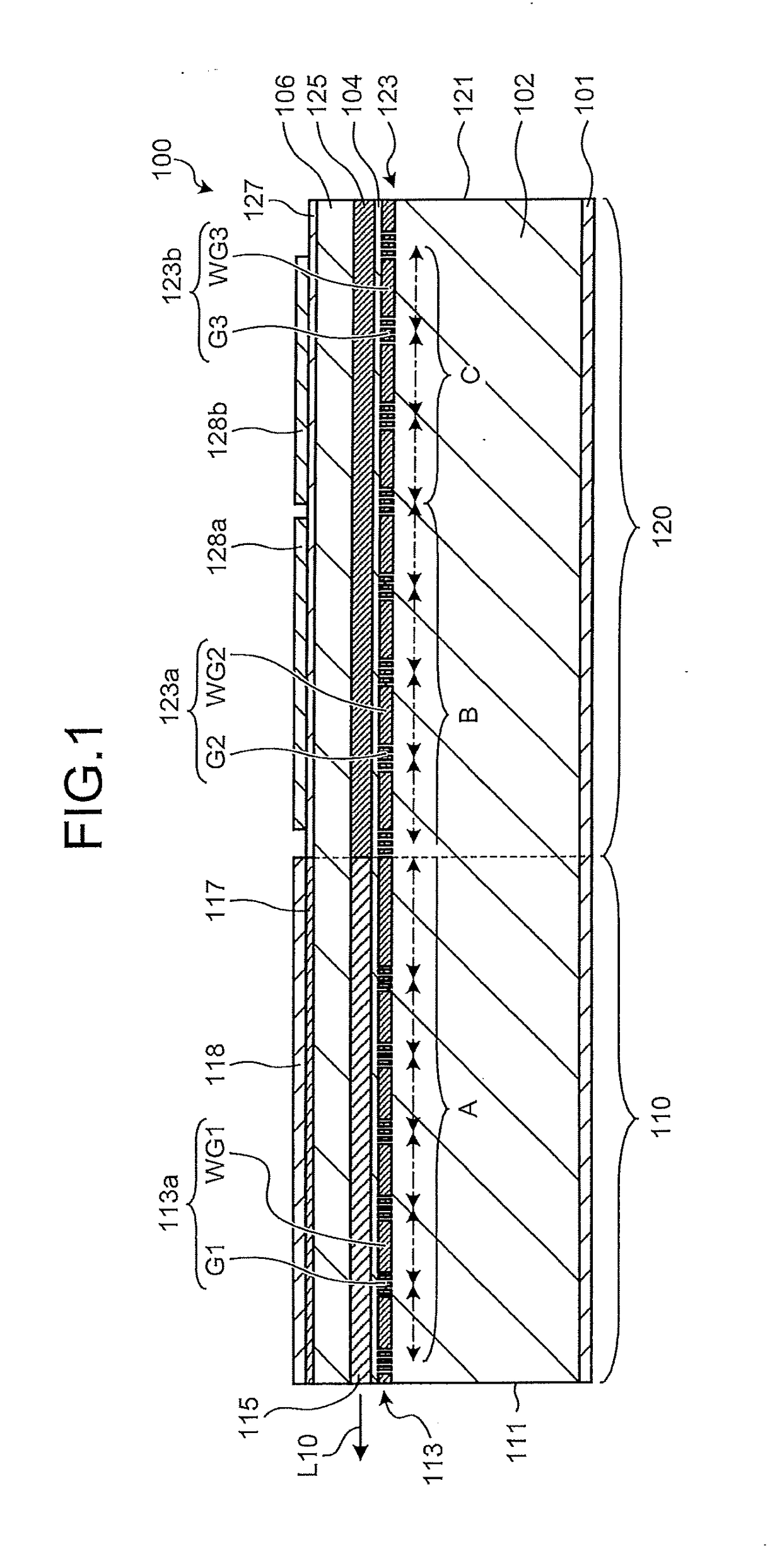
[0043]FIG. 1 is a schematic cross-sectional view of a semiconductor laser device according to a first embodiment of the present disclosure cut along an optical waveguide direction (lateral direction of the paper). As illustrated in FIG. 1, a semiconductor laser device 100 includes a gain SG section 110 which is an SG-DFB section having a waveguide core layer 115, which is an active layer that emits light by current injection, and a passive SG section 120 which is a CSG-DBR section that is adjacent to the gain SG section 110 and has a waveguide core layer 125 which is a passive waveguide core layer. An anti-reflection film (not illustrated) is formed on facets 111 and 121 of the gain SG section 110 and the passive SG section 120, respectively.

[0044]In addition, the semiconductor laser device 100 includes: an n-type semiconductor layer 102 having an n-side electrode 101 formed on a back face thereof; a diffraction grating layer 113 formed on the n-type semiconductor layer 102 in the g...

second embodiment

[0099]A diffraction grating structure according to a designing method according to one aspect of the present disclosure is not applicable only to the CSG-DR laser. The diffraction grating structure can be applied to improve performance of various semiconductor optical devices if utilizing a characteristic that an arbitrary reflection spectrum can be easily realized.

[0100]FIG. 16 is a schematic cross-sectional view of a semiconductor laser device according to a second embodiment cut along an optical waveguide direction. A semiconductor laser device 200 is called an inner grating multimode (iGM) laser having a partial diffraction grating inside the device (FURUKAWA ELECTRIC REVIEW No. 112 (July 2003), from pp. 5).

[0101]The semiconductor laser device 200 includes: an n-type semiconductor layer 202 having an n-side electrode 201 formed on a back face thereof; an active layer 203 formed on the n-type semiconductor layer 202; a p-type upper cladding layer 204 formed on the active layer 20...


PUM


Abstract

A semiconductor laser device is a vernier-type wavelength-tunable semiconductor laser device including an optical resonator, constituted by first and second reflective elements having reflection comb spectra in which reflection peaks are arranged on a wavelength axis in a substantially periodic manner and having mutually different periods. At least one of the first and second reflective elements has a sampled grating structure having a reflection comb spectrum in which reflection phases at the respective reflection peaks are aligned and the intensity of a reflection peak outside a set laser emission wavelength bandwidth is lower than the intensity of a reflection peak within the laser emission wavelength bandwidth.

Description

CROSS-REFERENCE TO RELATED APPLICATION(S)[0001]This application is a continuation of International Application No. PCT / JP2017 / 005166, filed on Feb. 13, 2017 which claims the benefit of priority of the prior Japanese Patent Application No. 2016-025315, filed on Feb. 12, 2016, the entire contents of which are incorporated herein by reference.BACKGROUND OF THE INVENTION1. Field of the Invention[0002]The present disclosure relates to a semiconductor laser device, a diffraction grating structure, and a diffraction grating.2. Description of the Related Art[0003]In the past, a wavelength-tunable laser device has been used which is obtained by combining two reflective elements. Each of the reflective elements has a reflection comb spectrum in which reflection peaks are arranged substantially in a periodic manner on a wavelength axis. If two reflective elements are used in combination in which wavelength intervals between reflection peaks in the reflection comb spectra are slightly different...

Claims


Application Information

Patent Timeline
Patent Type & Authority Applications(United States)
IPC IPC(8): H01S5/12H01S5/343H01S5/06
CPCH01S5/1209H01S5/3434H01S5/1237H01S5/0612H01S5/0261H01S2301/176H01S5/1215H01S5/06256
Inventor KIYOTA, KAZUAKIKAWAKITA, YASUMASA
Owner FURUKAWA ELECTRIC CO LTD
Why Eureka
Try Eureka