Package substrate and package structure

a technology of package substrate and package structure, which is applied in the direction of semiconductor devices, semiconductor/solid-state device details, electrical apparatus, etc., can solve the problems of inability to support such high-density wiring schemes, difficulty in keeping the manufacturing process simple, etc., and achieves low warpage, good mechanical stability, and high quality of electrical signal transmission.

Active Publication Date: 2018-12-06
HU DYI CHUNG
View PDF35 Cites 5 Cited by
  • Summary
  • Abstract
  • Description
  • Claims
  • Application Information

AI Technical Summary

Benefits of technology

The invention provides a package substrate and package structure with high-density interconnections that have good electrical signal transmission and low warping. The package substrate includes fine redistribution circuitry and first redistribution circuitry without the use of foreign materials like solders, making it a reliable interconnection structure. The mechanical stability of the package substrate is reinforced by the higher Young's modulus of the core compared to the first redistribution circuitry.

Problems solved by technology

However, conventional types of package substrate using build-up circuit structures are not able to support such high-density wiring schemes.
Therefore, fabricating a package substrate that has a high-density interconnection while keeping the manufacturing process simple has become a challenge to researchers in the field.

Method used


Image

  • Package substrate and package structure
  • Package substrate and package structure
  • Package substrate and package structure

Examples


Embodiment Construction

[0016]Reference will now be made in detail to the present preferred embodiments of the invention, examples of which are illustrated in the accompanying drawings. Wherever possible, the same reference numbers are used in the drawings and the description to refer to the same or like parts.

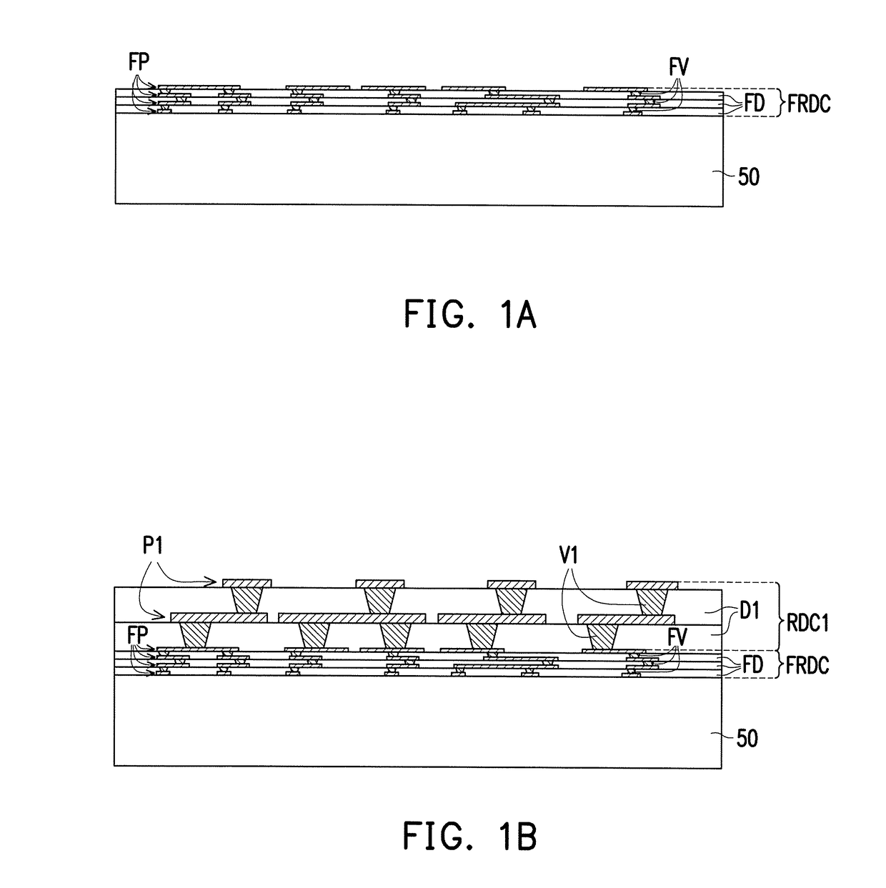
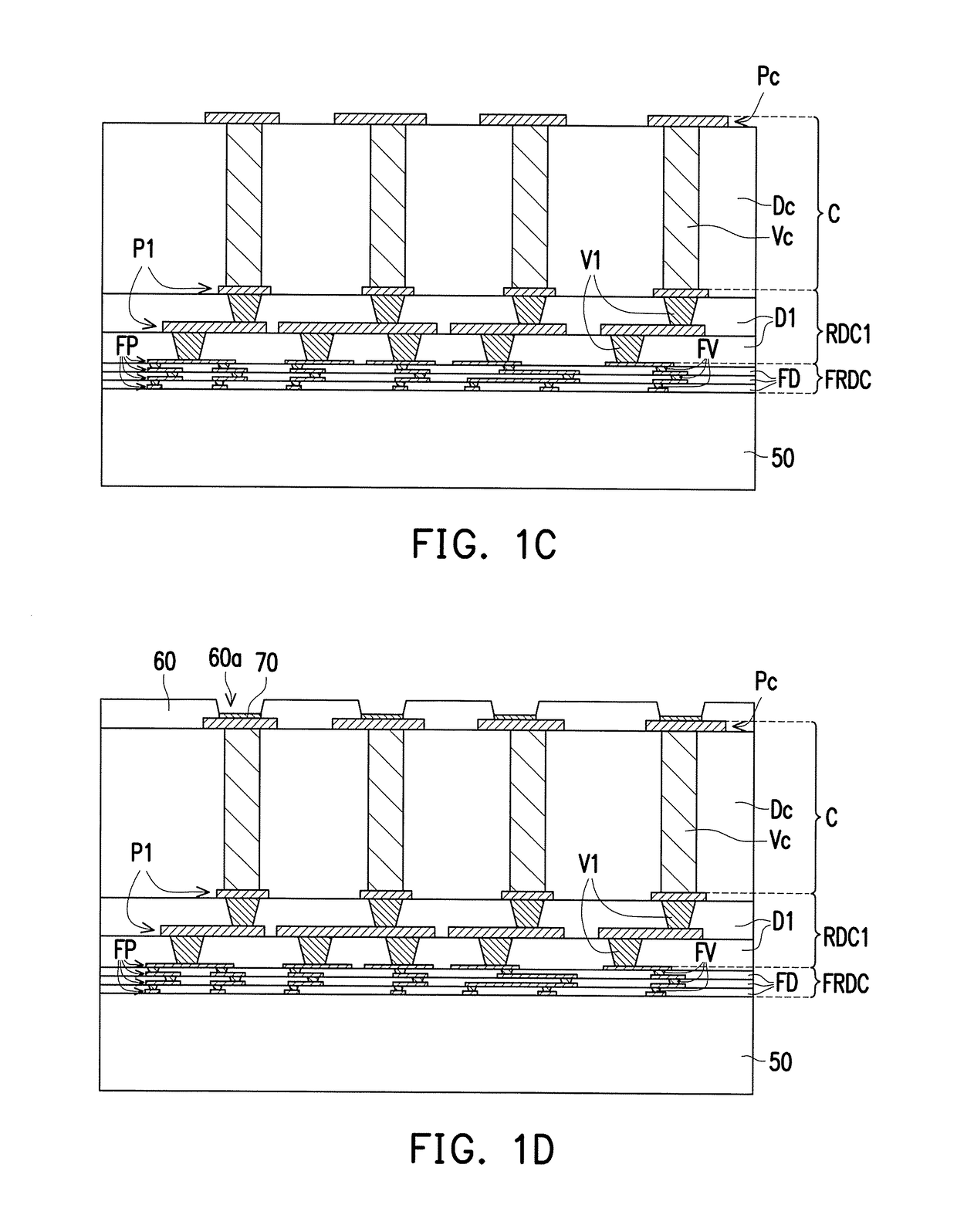
[0017]The following describes a manufacturing method of a package substrate with reference to FIGS. 1A to 2. FIGS. 1A to 1E are schematic cross-sectional views illustrating a manufacturing method of a package substrate according to an embodiment of the invention. FIG. 2 is a schematic cross-sectional view illustrating a fine conductive via and a first conductive via according to an embodiment of the invention. Referring to FIG. 1 A first, a fine redistribution circuitry FRDC including a fine conductive pattern FP, a fine dielectric layer FD and a fine conductive via FV is formed on a temporary carrier 50. In some embodiments, the fine conductive pattern FP is stacked on the fine dielectric layer FD. ...


PUM


Abstract

A package substrate including a fine redistribution circuitry, a first redistribution circuitry disposed on the fine redistribution circuitry and a core disposed on the first redistribution circuitry opposite to the fine redistribution circuitry. The fine redistribution circuitry includes a fine conductive pattern. The first redistribution circuitry includes a first conductive pattern electrically connected to the fine conductive pattern. A thickness of the fine redistribution circuitry is less than a thickness of the first redistribution circuitry and a dimension of the fine conductive pattern is less than a dimension of the first conductive pattern. The core is electrically connected to the first conductive pattern. The Young's modulus of the core is greater than the Young's modulus of the first redistribution circuitry. A package structure is also provided.

Description

CROSS REFERENCE TO RELATED APPLICATION[0001]This application claims the priority benefit of U.S. provisional application Ser. No. 62 / 512,731, filed on May 31, 2017. The entirety of the above-mentioned patent application is hereby incorporated by reference herein and made a part of the specification.BACKGROUND OF THE INVENTION1. Field of the Invention[0002]The present invention relates to an electronic package technology, and more specifically relates to a package substrate and a package structure employing such the package substrate.2. Description of Related Art[0003]As the electronic industry has rapidly developed, the trend in electronic products has been to gradually move toward multi-functionality and high performance. One of the conventional structures of semiconductor packages has a semiconductor chip mounted on a package substrate which includes a core with symmetric built-up circuit structures.[0004]In order to meet the demand for greater integration and miniaturization with...

Claims


Application Information

Patent Timeline
Patent Type & Authority Applications(United States)
IPC IPC(8): H01L23/498H01L21/48H01L21/683
CPCH01L23/49822H01L21/4857H01L21/6835H01L23/49838H01L23/49894H01L2221/68345H01L2224/16225H01L2924/15311H01L23/3128H01L23/49827H01L23/49816
Inventor HU, DYI-CHUNG
Owner HU DYI CHUNG
Why Eureka
Try Eureka