Automated method for integrated analysis of back end of the line yield, line resistance/capacitance and process performance

a technology of line yield and process performance, applied in the direction of knowledge representation, semiconductor/solid-state device testing/measurement, instruments, etc., can solve the problems of billions of dollars in capital investment and maintenance expenses

Active Publication Date: 2018-12-06
IBM CORP
View PDF2 Cites 3 Cited by
  • Summary
  • Abstract
  • Description
  • Claims
  • Application Information

AI Technical Summary

Benefits of technology

The patent describes a method and system for analyzing the dimensions and electrical performance of semiconductor device manufacturing structures. This analysis is done by measuring the dimensions of the structures and comparing them to a process outlook model to determine any variations. The system then uses machine learning to apply scenarios for process modifications to the structure based on the variations and electrical measurements. The method and system can help improve the manufacturing process for semiconductor devices.

Problems solved by technology

The semiconductor industry has been characterized by sophisticated high-tech equipment, a high degree of factory automation, and ultra-clean manufacturing facilities that cost billions of dollars in capital investment and maintenance expense.

Method used


Image

  • Automated method for integrated analysis of back end of the line yield, line resistance/capacitance and process performance
  • Automated method for integrated analysis of back end of the line yield, line resistance/capacitance and process performance
  • Automated method for integrated analysis of back end of the line yield, line resistance/capacitance and process performance

Examples


Embodiment Construction

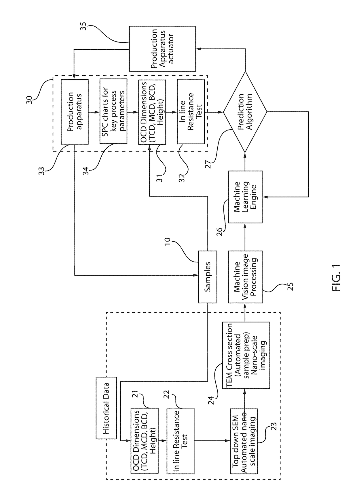
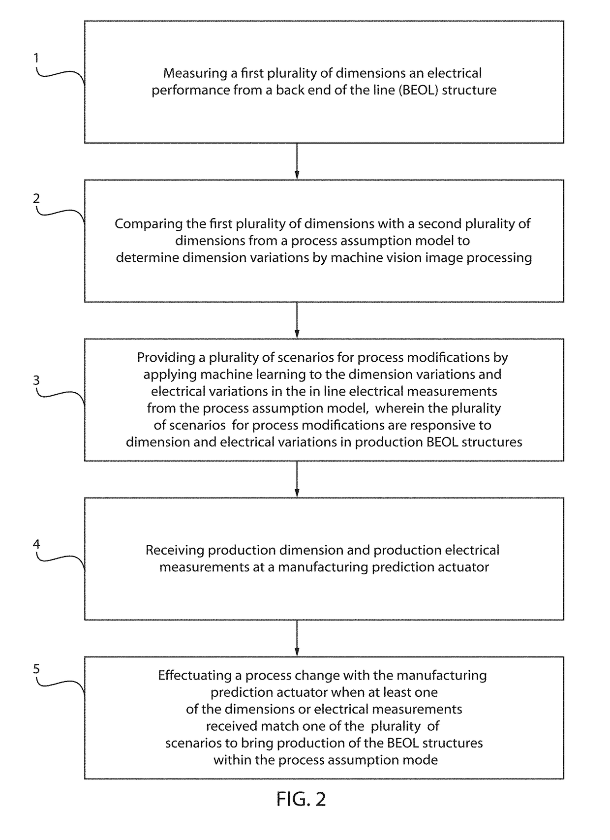
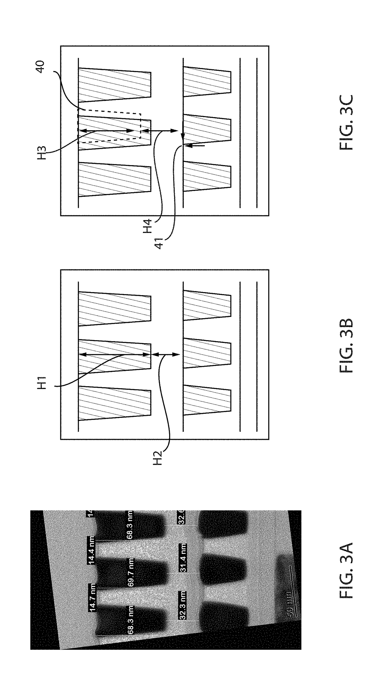
[0022]In semiconductor manufacturing rapid cost and effective analysis of back end of the line (BEOL) resistance and yield variation is needed. Currently, chip yield and performance parameters are correlated to structural changes, metrology data (defects) and process parameters manually. The analysis process is slow, inefficient and labor intensive. Manual intervention by engineers can occur at several steps. In some embodiments, the methods, systems and computer program products provided herein may provide a faster and more efficient method of back end of the line (BEOL) analysis of semiconductor device manufacturing using automated sample preparation, automated image processing, and machine learning algorithms to correlate process parameters to back end of the line (BEOL) interconnect performance parameters, such as resistance and yield, changes in the geometry of metal lines and metal line related structures, and other metrology data. Exemplary applications / uses to which the pres...


PUM


Abstract

A method of electrical device manufacturing that includes measuring a first plurality of dimensions and electrical performance from back end of the line (BEOL) structures; and comparing the first plurality of dimensions with a second plurality of dimensions from a process assumption model to determine dimension variations by machine vision image processing. The method further includes providing a plurality of scenarios for process modifications by applying machine image learning to the dimension variations and electrical variations in the in line electrical measurements from the process assumption model. The method further includes receiving production dimension measurements and electrical measurements at a manufacturing prediction actuator. The at least one of the dimensions or electrical measurements received match one of the plurality of scenarios the manufacturing prediction actuator using the plurality of scenarios for process modifications effectuates a process change.

Description

BACKGROUNDTechnical Field[0001]The present invention generally relates to semiconductor manufacturing, and more particularly to process control techniques for semiconductor manufacturing processes.Description of the Related Art[0002]The semiconductor industry has been characterized by sophisticated high-tech equipment, a high degree of factory automation, and ultra-clean manufacturing facilities that cost billions of dollars in capital investment and maintenance expense. In order to achieve acceptable yield and device performance levels, very tight process specifications must be achieved.SUMMARY[0003]In one embodiment, a method of automated back end of the line (BEOL) analysis of semiconductor device manufacturing is provided that may include measuring a first plurality of dimensions from a back end of the line (BEOL) structure of an electrical device and electrical performance of the BEOL structure; and comparing the first plurality of dimensions with a second plurality of dimensio...

Claims


Application Information

Patent Timeline
Patent Type & Authority Applications(United States)
IPC IPC(8): G06F17/50G06N5/02H01L21/66
CPCG06F2217/12G06N5/025G06F17/5036H01L22/20G06F17/5081H01L22/12H01L22/14G06N20/00G06F30/367G06F30/398G06F2119/18
Inventor BHOSALE, PRASADRIZZOLO, MICHAELYANG, CHIH-CHAO
Owner IBM CORP
Why Eureka
Try Eureka