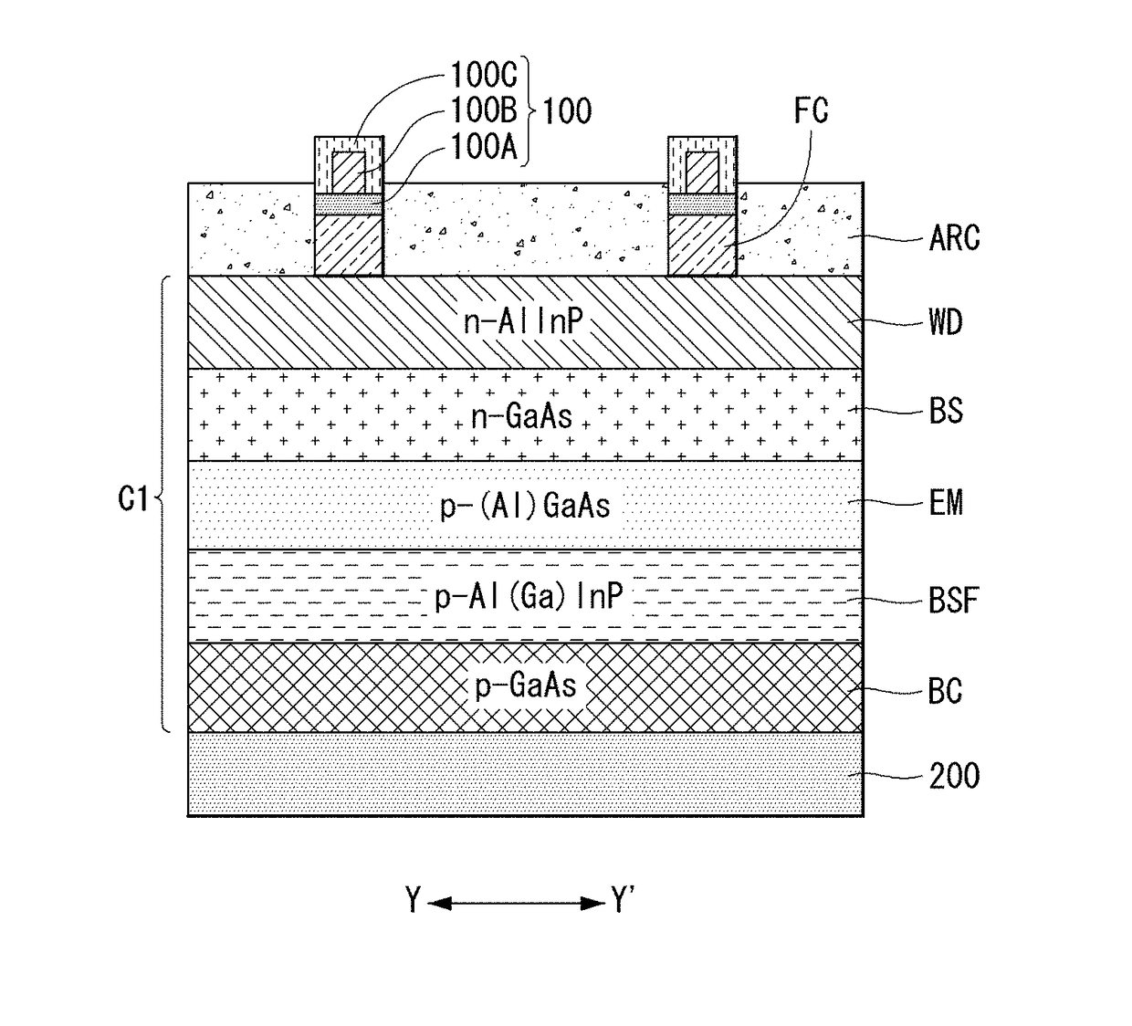
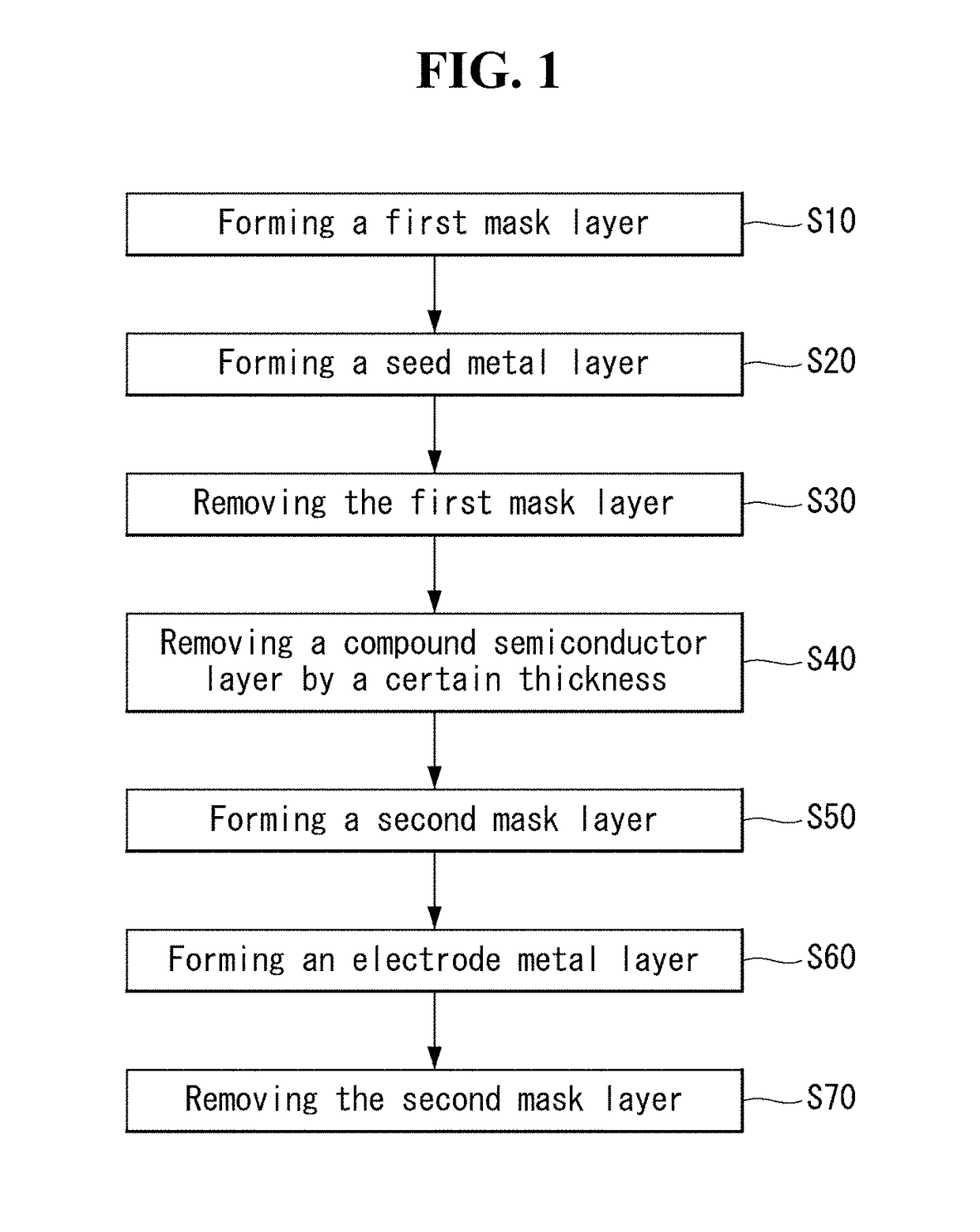
Compound semiconductor solar cell and method of manufacturing the same
a technology of solar cells and semiconductors, applied in the field can solve the problems of difficult to lower the manufacturing cost of compound semiconductor solar cells, and achieve the effects of reducing material costs, preventing damage and performance deterioration of compound semiconductor layers, and reducing material costs
- Summary
- Abstract
- Description
- Claims
- Application Information
AI Technical Summary
Benefits of technology
Problems solved by technology
Method used
Image


Examples
Embodiment Construction
[0035]Reference will now be made in detail embodiments of the disclosure examples of which are illustrated in the accompanying drawings. Since the present disclosure may be modified in various ways and may have various forms, specific embodiments are illustrated in the drawings and are described in detail in the present specification. However, it should be understood that the present disclosure are not limited to specific disclosed embodiments, but include all modifications, equivalents and substitutes included within the spirit and technical scope of the present disclosure.
[0036]The terms “first”, “second”, etc. may be used to describe various components, but the components are not limited by such terms. The terms are used only for the purpose of distinguishing one component from other components.
[0037]For example, a first component may be designated as a second component, and a second component may be designated as a first component without departing from the scope of the present ...
PUM
 Abstract
Description
Claims
Application Information
 - R&D
- Intellectual Property
- Life Sciences
- Materials
- Tech Scout
- Unparalleled Data Quality
- Higher Quality Content
- 60% Fewer Hallucinations
Browse by: Latest US Patents, China's latest patents, Technical Efficacy Thesaurus, Application Domain, Technology Topic, Popular Technical Reports.
© 2025 PatSnap. All rights reserved.Legal|Privacy policy|Modern Slavery Act Transparency Statement|Sitemap|About US| Contact US: help@patsnap.com