Method for producing a radiation detector and radiation detector

a radiation detector and detector technology, applied in the direction of final product manufacturing, sustainable manufacturing/processing, instruments, etc., can solve the problems of not being able and/or affordable, not yet known how to efficiently grow a thick (poly) crystalline layer on a substrate, and not being able to achieve the effect of high quantum efficiency, fast temporal response and reduced production costs

Active Publication Date: 2018-09-27
KONINKLJIJKE PHILIPS NV
View PDF0 Cites 6 Cited by
  • Summary
  • Abstract
  • Description
  • Claims
  • Application Information

AI Technical Summary

Benefits of technology

[0015]Furthermore, it is found that the inorganic-organic halide Perovskite materials need not to be provided in the form of single crystals, which allows for reductions in production costs.
[0016]It is further found that desirable properties such as high quantum efficiency, fast temporal response, high radiation resistance, thermal and chemical stability are possible.
[0017]The present inventions allows for layers that can be made quite thick with only moderate electric fields needed due to good charge mobility properties.

Problems solved by technology

Growing single crystals is known, however it is not yet known how to efficiently grow a thick (poly) crystalline layer on a substrate.
For layers above 10 μm thick this is not possible and / or affordable.

Method used


Image

  • Method for producing a radiation detector and radiation detector
  • Method for producing a radiation detector and radiation detector
  • Method for producing a radiation detector and radiation detector

Examples


Embodiment Construction

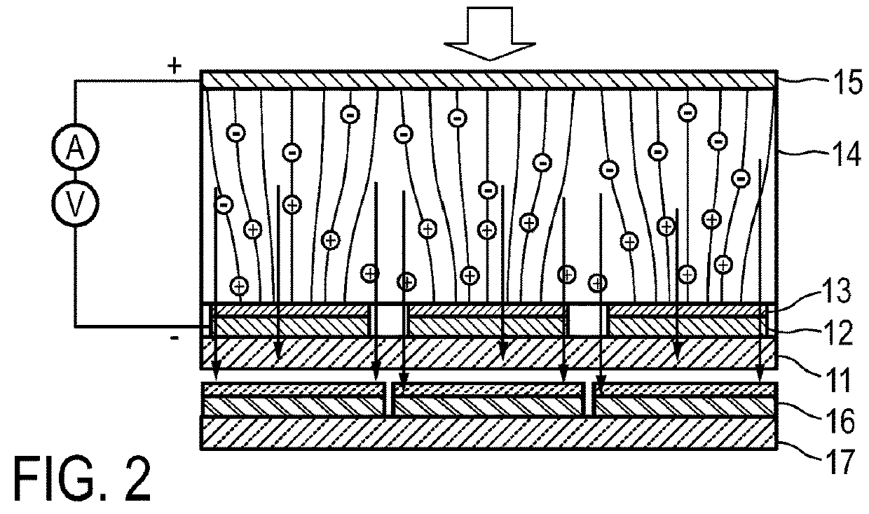
[0056]FIG. 1 shows a schematic diagram of a radiation detector in accordance with an embodiment of the invention.

[0057]The basic structure includes a substrate 1 with structured bottom electrodes 2 on it. On top of the bottom electrode 2 an electron blocking layer (not shown) might be present. On top of the arrangement of substrate 1 and bottom electrodes 2 a halide Perovskite layer 4 is placed, with a seeding layer 3 provided on the bottom electrodes 2. This layer 4 might be thin (100 nm-100 μm) for mammography, thicker (100-2000 μm) for general X-ray and CT and quite thick (1-20 mm) for SPECT or PET.

[0058]On top of layer 4 a hole blocking layer might (not shown) be present. Also might there be a conducting layer (not shown) to reduce / prevent shorts of a top electrode 5 towards the substrate 1.

[0059]On top of the above mentioned layers, the top electrode 5 is deposited. The top electrode 5 might contain an electron injection layer (not shown).

[0060]Preferably the total structure is...


PUM


Abstract

The invention relates to a method for producing a radiation detector used to detect ionizing radiation including a first inorganic-organic halide Perovskite material (24) as a direct converter material and/or as a scintillator material in a detector layer and to a radiation detector comprising a detector layer (24) produced by means of the steps of the method. In order to provide an approach for producing a thick layer (e.g. above 10 μιη) of Perovskite material suitable for a radiation detector, it is proposed to grow the material selectively on a seeding layer (23), yielding in a thick polycrystalline layer. One suitable seeding layer (23) to grow lead Perovskite material is made of a bromide Perovskite material.

Description

FIELD OF THE INVENTION[0001]The invention relates to a method for producing a radiation detector for ionizing radiation including a first inorganic-organic halide Perovskite material as a direct converter material and / or as a scintillator material in a detector layer and to a radiation detector comprising a detector layer produced by means of the steps of the method.BACKGROUND OF THE INVENTION[0002]Scintillators are materials that absorb high energy radiation, such as α-, β, γ-rays, X-rays, neutrons or other high energetic particles, and convert that energy into bursts of visible photons. In detectors for the above mentioned radiation, these photons are then converted into electrical pulses by photo-detectors.[0003]Alternatively the radiation is converted directly in a semiconductor which is sandwiched between two electrodes. In a detector the initially created electron-hole-pairs are separated by an externally applied electric field and the resulting electrical current sensed by an...

Claims


Application Information

Patent Timeline
Patent Type & Authority Applications(United States)
IPC IPC(8): H01L27/30G01T1/20G01T1/202G01T1/24H01L51/42H01L51/00H01L51/44
CPCH01L27/308G01T1/2018G01T1/2023G01T1/241H01L51/4273H01L51/0003H01L51/441H01L51/0077G01T1/24Y02E10/549Y02P70/50H10K39/36H10K85/50H10K30/81H10K30/353H10K71/12H10K85/30
Inventor LIFKA, HERBERTBAKEN, JOANNA MARIA ELISABETHCOEHOORN, REINDERVAN HAL, PAULUS ALBERTUSWIECZOREK, HERFRIED KARLHUMMEL, HELGARONDA, CORNELIS REINDERSIMON, MATTHIAS
Owner KONINKLJIJKE PHILIPS NV
Why Eureka
Try Eureka