
In-cell touch display device and related test system and test method

a touch display device and in-cell technology, applied in the direction of instruments, error detection/correction, computing, etc., can solve the problems of in-cell touch display device not working properly inability to test, etc., to achieve the effect of reducing testing cost and time, reducing testing costs

Inactive Publication Date: 2018-09-27
HANNSTAR DISPLAY NANJING +1
View PDF4 Cites 18 Cited by
  • Summary
  • Abstract
  • Description
  • Claims
  • Application Information

AI Technical Summary

Benefits of technology

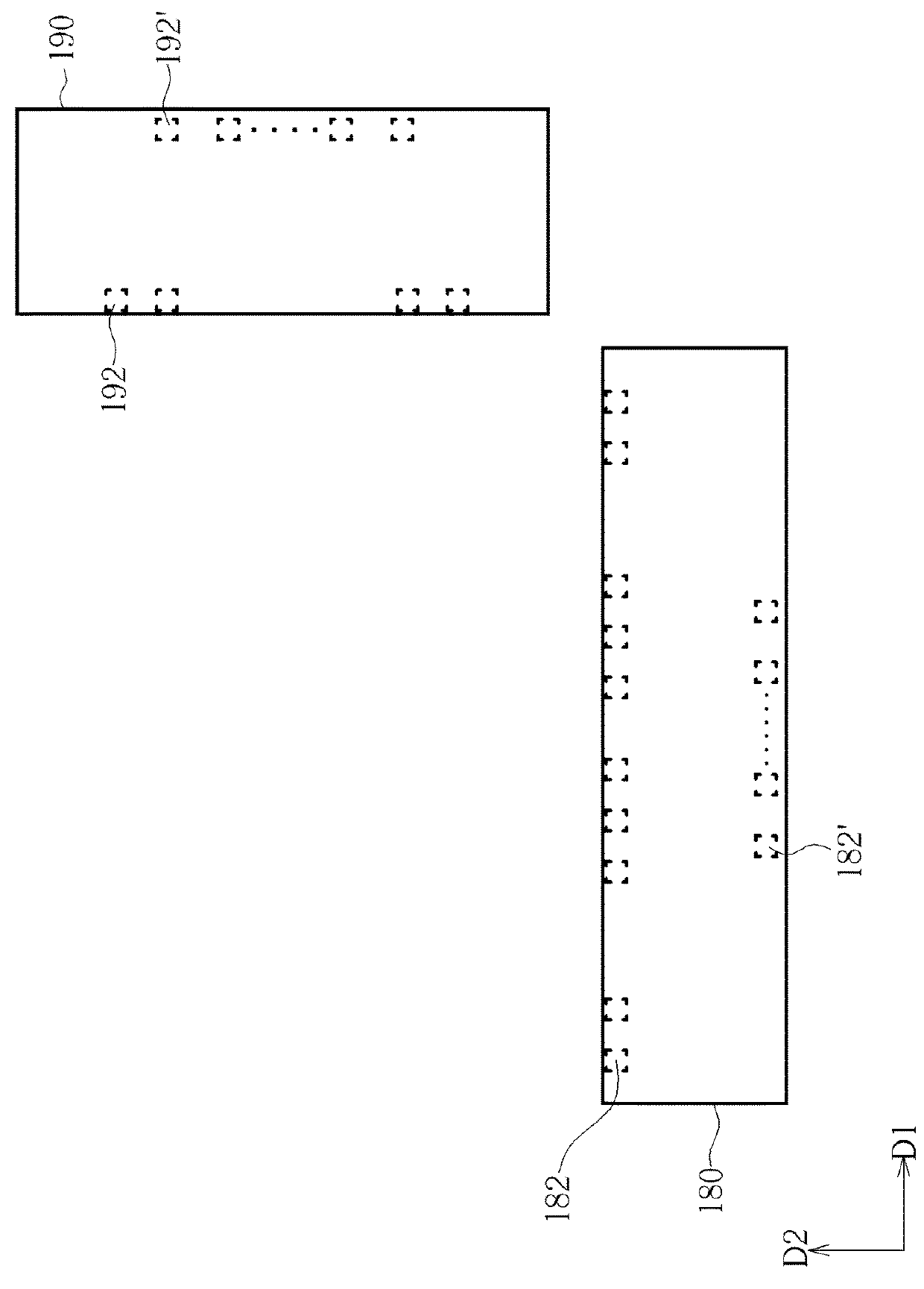
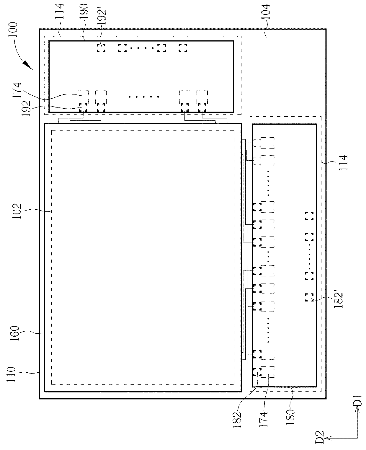
The in-cell touch display device test system described in this patent text has several technical effects. First, the size of the connection pads is increased, which reduces misalignment and alignment time between the conductive pins of the test plate and the corresponding connection pads, providing more convenience and accuracy in the testing process. Second, the connection pads have extension parts that can be placed in the bonding area, which allows for the arrangement of these parts without increasing the size of the peripheral region and maintaining the size of the product and display area. This also helps in economizing the testing cost and time. Third, the test system allows for independent testing of the display and touch functions, without interfering with each other. Fourth, the test system provides the same test signals as the integrated circuit chip, allowing for full contact testing of the touch sensing function and display function of the in-cell touch display device. This helps in identifying any potential issues with the function of the device before connecting it to the integrated circuit chip.

Problems solved by technology

However, in the manufacturing process of the in-cell touch display device, defects generated in the manufacturing process can cause the in-cell touch display device to not work properly.
But, because these methods need to further dispose testing lines of testing thin film transistors, the load of circuit in the in-cell touch display device would be affected, so as to influence a touch sensing function, a display function and manufacturing cost of the in-cell touch display device, wherein the larger size of the in-cell touch display device is particularly affected.

Method used


Image

  • In-cell touch display device and related test system and test method
  • In-cell touch display device and related test system and test method
  • In-cell touch display device and related test system and test method

Examples


Embodiment Construction

[0047]To provide a better understanding of the present invention to the skilled users in the technology of the present invention, preferred embodiments will be detailed as follows. The preferred embodiments of the present invention are illustrated in the accompanying drawings with numbered elements to elaborate on the contents and effects to be achieved. It is needed to note that the drawings are simplified schematic, and therefore, the drawings show only the components and combinations associated with the present invention, so as to provide a clearer description of the basic architecture or method of implementation of the present invention. The components would be complex in reality. In addition, in order to explain, the components shown in the drawings of the present invention are not drawn to the actual number, shape, and dimensions, the detail can be adjusted according to the design requirements.

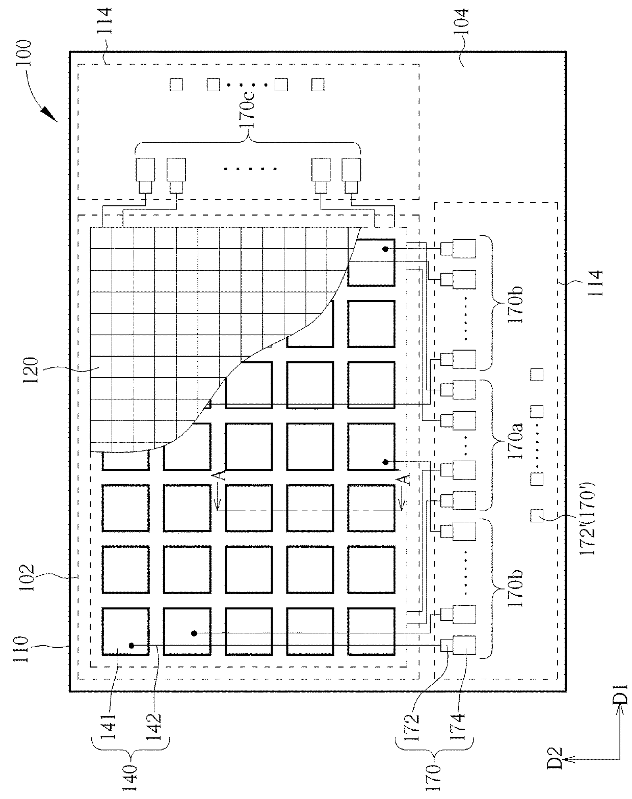
[0048]FIG. 1 to FIG. 2b are schematic diagrams of a top view of an in-cell touch dis...


PUM

PropertyMeasurementUnit
widthaaaaaaaaaa
lengthaaaaaaaaaa
areaaaaaaaaaaa

Abstract

An in-cell touch display device includes a first substrate, a second substrate, a plurality of scan lines, a plurality of data lines, a plurality of touch electrodes and a plurality of connection pads. The second substrate is disposed opposite to the first substrate. The scan lines and the data lines are disposed on the first substrate. The touch electrodes are disposed between the first substrate and the second substrate. The connection pads are disposed on the first substrate, and the connection pads are electrically connected to one of the data lines or one of the touch electrodes. Each of at least some of the connection pads has a bonding part and an extension part, and an area of the bonding part is smaller than an area of the extension part.

Description

BACKGROUND OF THE INVENTION1. Field of the Invention[0001]The present invention relates to an in-cell touch display device, an in-cell touch display device test system and a test method of an in-cell touch display device, and more particularly to an in-cell touch display device, an in-cell touch display device test system and a test method of an in-cell touch display device for independently testing a touch sensing function and a display function.2. Description of the Prior Art[0002]In the various electronic products, a touch display device has been formed by a display screen with touch components extensively, such that users can directly communicate with the electronic products instead of the conventional input equipment such as keyboard and mouse, so as to decrease the size of the electronic products and improve the convenience of communication between human and machines. Nowadays, the industry is currently committed to developing an in-cell touch display device in which the touch...

Claims


Application Information

Patent Timeline
Patent Type & Authority Applications(United States)
IPC IPC(8): G09G3/00G06F3/041G02F1/1333G09G3/36
CPCG09G3/006G06F3/0412G09G2300/0426G09G3/3674G02F1/13338G06F3/04164G06F3/0443G02F1/1309G02F1/13458G06F11/2221G06F3/0446
Inventor LEE, HSING-YINGLIN, SUNG-CHUNTSAI, JUI-HSIN
Owner HANNSTAR DISPLAY NANJING
Learn More