
Semiconductor apparatus and method for preparing the same

a technology of semiconductor devices and lateral protrusions, which is applied in the direction of electrical apparatus, semiconductor/solid-state device details, semiconductor devices, etc., can solve the problems of poor electrical interconnection, complex manufacturing of semiconductor devices, and increasing the complexity of semiconductor devices, so as to achieve the effect of eliminating the failure of the electrical function due to lateral protrusion and the higher thermal expansion coefficien

Inactive Publication Date: 2018-08-16
NAN YA TECH
View PDF1 Cites 5 Cited by
  • Summary
  • Abstract
  • Description
  • Claims
  • Application Information

AI Technical Summary

Benefits of technology

The present patent is about a semiconductor device that has multiple semiconductor devices fused together using a fusion bonding technique. The semiconductor devices have conductive portions that have a higher coefficient of thermal expansion than their dielectric portions. By creating a space for the conductive portion to expand during the fusion bonding process, the semiconductor device does not have any protrusions that could damage the interface between the two dielectric portions. This results in a more reliable electrical function.

Problems solved by technology

The patent text discusses the challenges of manufacturing semiconductor devices in a miniaturized scale, which can result in poor electrical interconnection, cracks, and delamination of components. The technical problem addressed in the patent is to modify the structure and manufacture of semiconductor devices to overcome these challenges.

Method used


Image

  • Semiconductor apparatus and method for preparing the same
  • Semiconductor apparatus and method for preparing the same
  • Semiconductor apparatus and method for preparing the same

Examples


Embodiment Construction

[0032]The following description of the disclosure accompanies drawings, which are incorporated in and constitute a part of this specification, and which illustrate embodiments of the disclosure, but the disclosure is not limited to the embodiments. In addition, the following embodiments can be properly integrated to complete another embodiment.

[0033]References to “one embodiment,”“an embodiment,”“exemplary embodiment,”“other embodiments,”“another embodiment,” etc. indicate that the embodiment(s) of the disclosure so described may include a particular feature, structure, or characteristic, but not every embodiment necessarily includes the particular feature, structure, or characteristic. Further, repeated use of the phrase “in the embodiment” does not necessarily refer to the same embodiment, although it may.

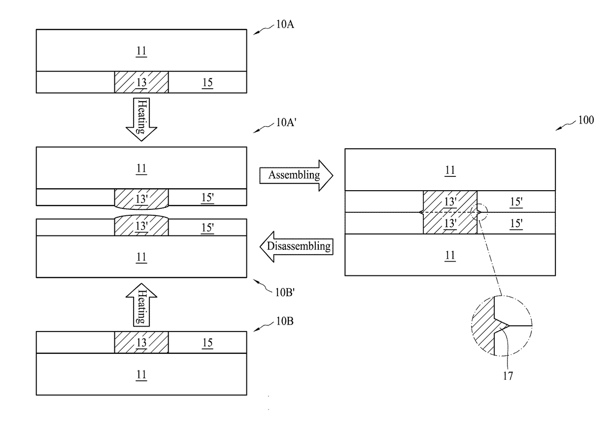
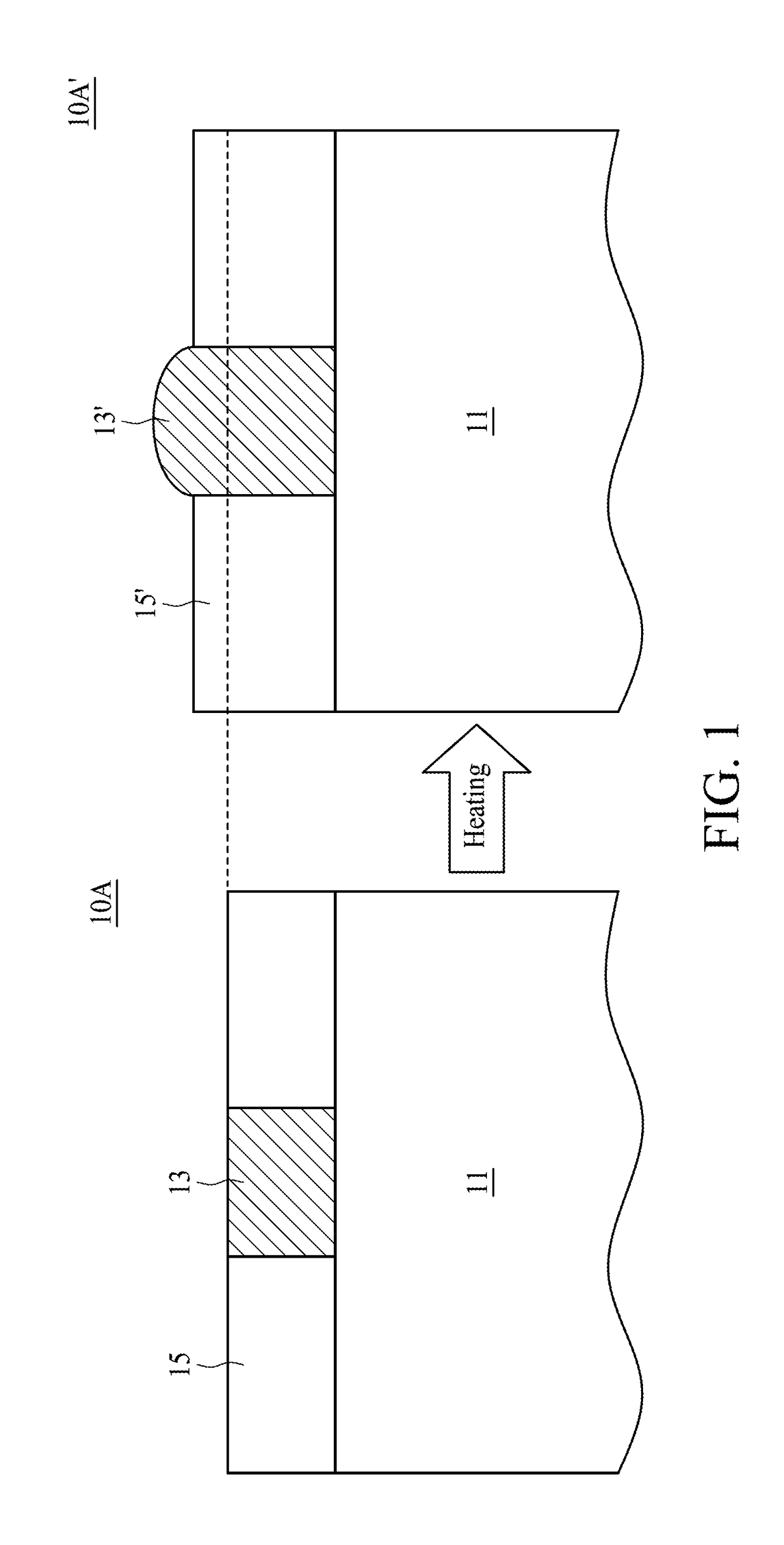
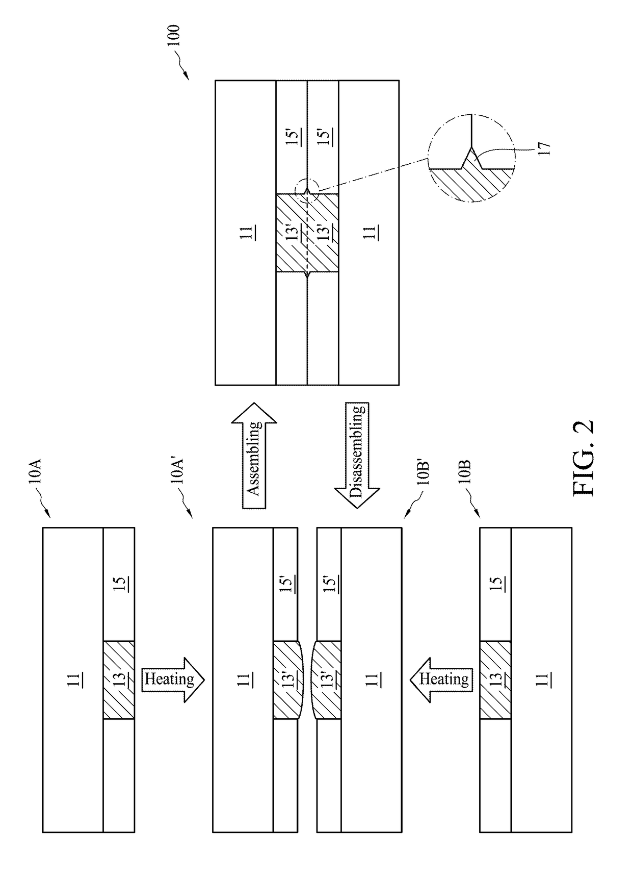
[0034]The present disclosure is directed to a semiconductor apparatus having a plurality of bonded semiconductor devices formed by a fusion bonding technique and a method for pre...


PUM


Abstract

The present disclosure is directed to a semiconductor apparatus having a plurality of bonded semiconductor devices formed by a fusion bonding technique and a method for preparing the same. The semiconductor devices have conductive portions with higher coefficient of thermal expansion than their dielectric portions. By forming the depression to provide a space for the volume expansion of the conductive portion with higher coefficient of thermal expansion during the subsequent thermal treating process of the fusion bonding, the semiconductor apparatus formed of semiconductor devices by the fusion bonding technique does not exhibit a lateral protrusion into the interface between the two dielectric portions. As a result, the failure of the electrical function due to the lateral protrusion is effectively eliminated.

Description


Claims


Application Information

Patent Timeline
Owner NAN YA TECH
Learn More